Explore five advanced vacuum deposition technologies used to engineer carbon, metal and compound thin films. See how each process works, compare the performance it can deliver and connect the right coating route to your application and production needs.
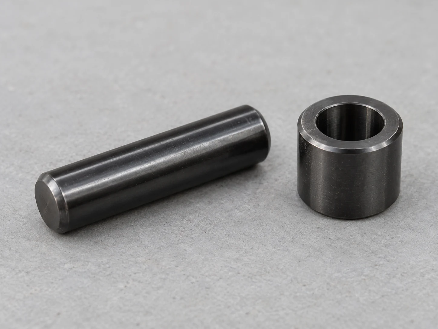
A steel guide pin can have the strength it needs and still wear where it slides against a bushing. A diamond-like carbon (DLC) coating can improve wear resistance and lower friction at that contact while the steel core carries the load.
Advanced thin film coatings add a layer of functional material, from nanometres to micrometres thick, while preserving the bulk properties of the component beneath. Engineers can select a coating for clean release from a mold or for corrosion protection on exposed metal. They can also tailor electrical behavior, optical response, surface energy and appearance to suit the application.
At NTI Nanofilm, we use physical vapor deposition (PVD) and plasma-enhanced chemical vapor deposition (PECVD) to deposit these films. The application guides our choice of carbon, metal, nitride, oxide, carbide or multilayer films. Both processes deposit the film in a vacuum, reducing reliance on the chemical baths and rinse water used in electroplating and anodising.
Explore application-specific solutions: PECVD DLC coatings · FCVA ta-C coatings.
PVD builds thin films from solid targets or cathodes using sputtering or arc based plasma. NTI PVD routes include Filtered Cathodic Vacuum Arc, Cathodic Arc Evaporation, Ion Beam Sputtering and Magnetron Sputtering.
PECVD forms coatings from plasma activated gaseous precursors, enabling hydrogenated DLC and related functional carbon films at substantially lower temperatures than conventional thermal CVD.
NTI Nanofilm brings FCVA, PECVD DLC, cathodic arc evaporation, ion beam sputtering and magnetron sputtering into one technology platform spanning ultra hard carbon, hard compounds, functional metals and precision multilayer films.
Carbon, metals, nitrides, oxides, carbides and multilayer architectures give engineers a broad film chemistry platform for wear, friction, release, electrical, optical, barrier and decorative performance.
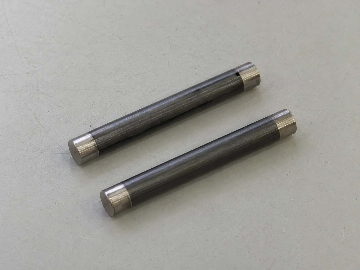
Hydrogen free ta-C, hydrogenated a-C:H and selected doped or hybrid carbon systems for hardness, low friction, wear control, release and electrical interface performance.
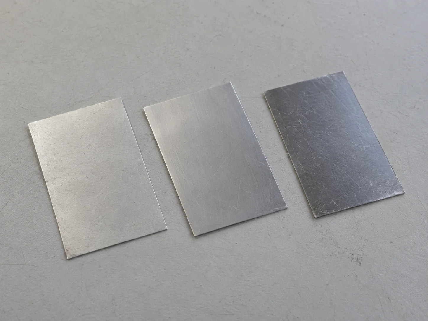
Hydrogen free ta-C, hydrogenated a-C:H and selected doped or hybrid carbon systems for hardness, low friction, wear control, release and electrical interface performance.
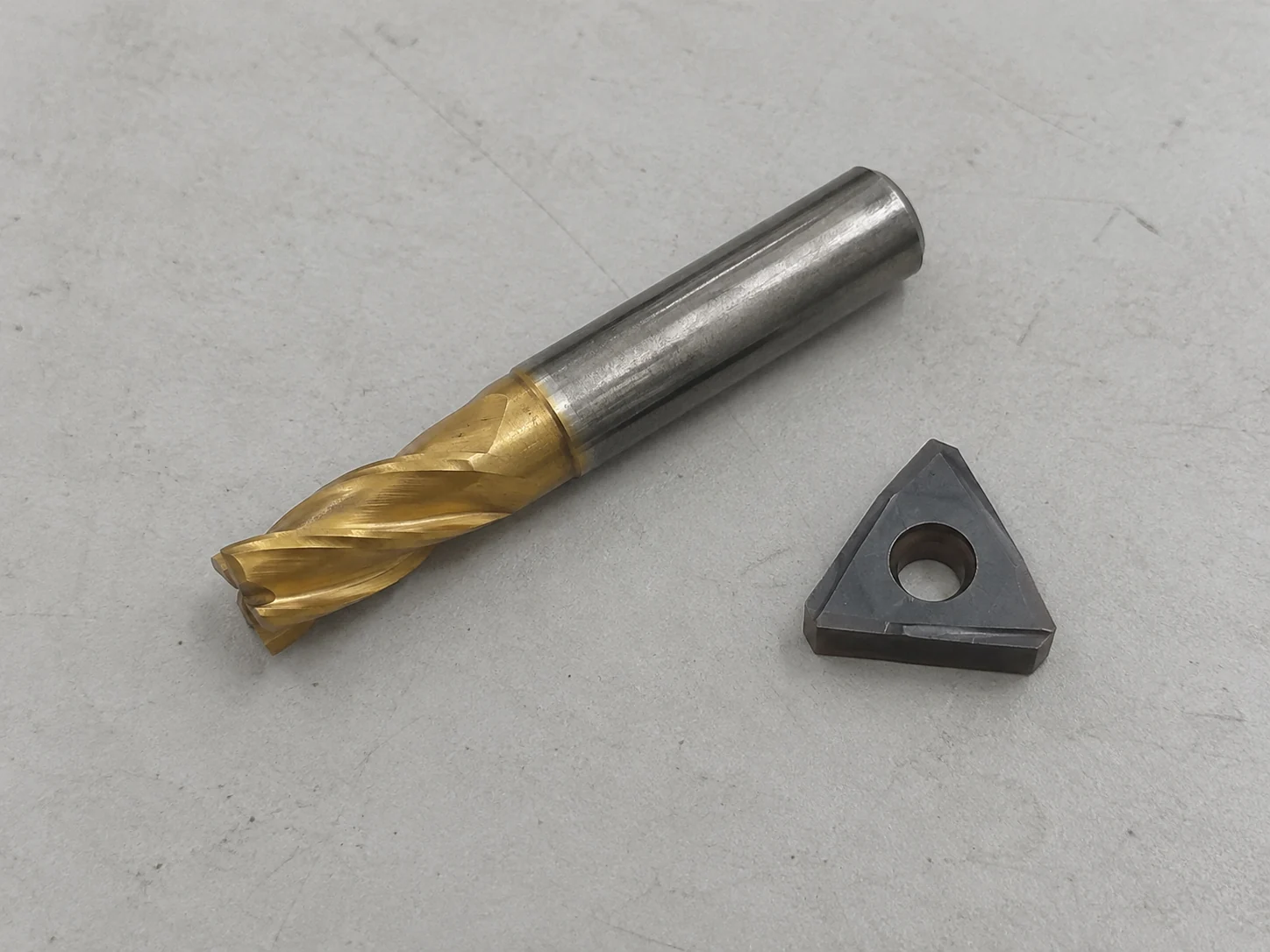
TiN, CrN, AlTiN, AlCrN, TiAlCrN and related nitride systems for hardness, wear resistance and high duty surface protection.
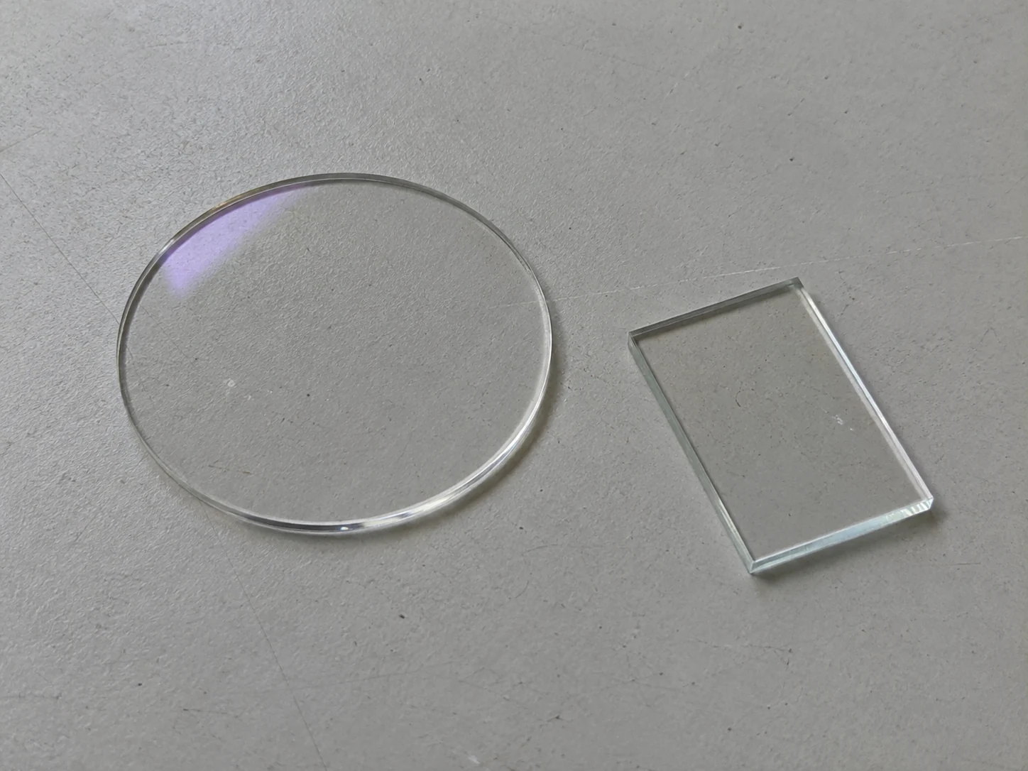
Selected metal oxide films for optical response, electrical insulation, barrier performance and functional surface control.
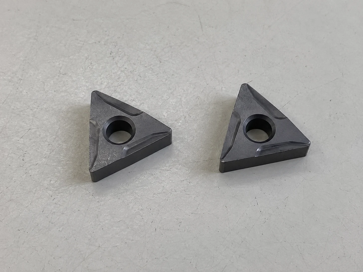
Selected carbide and carbonitride systems, including qualified TiCN and TiAlCN architectures, for wear resistance, friction control and demanding tooling applications.
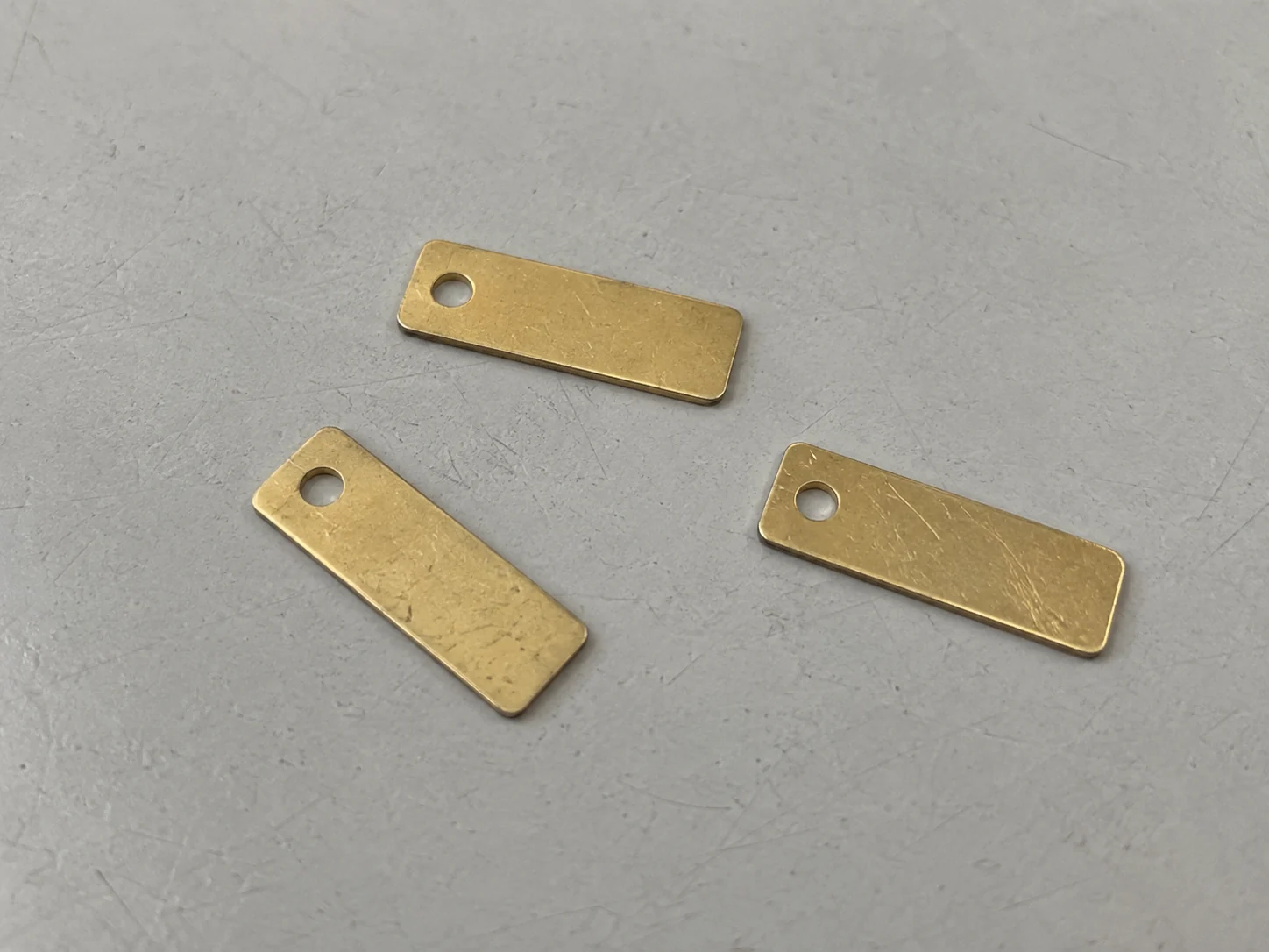
Selected precious and noble metal thin films for conductive interfaces, optical and electronic functions, corrosion control and premium appearance.
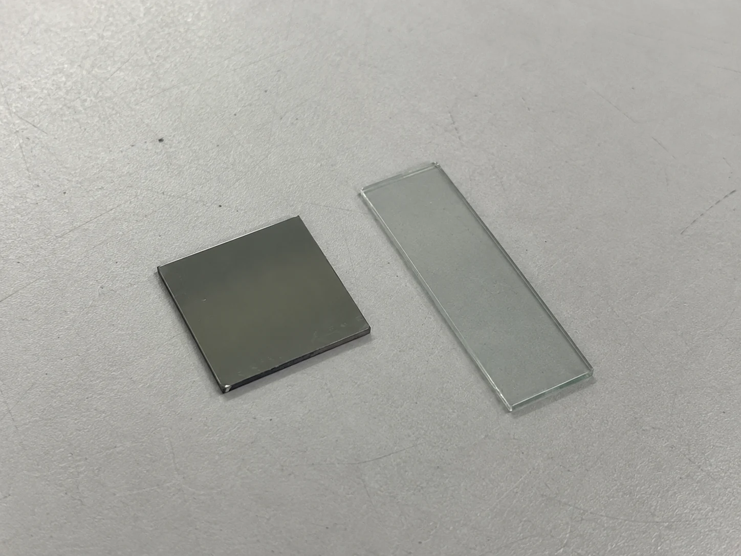
Reactive compound chemistries that tune optical, electrical, barrier and mechanical behaviour through controlled gas and material composition.
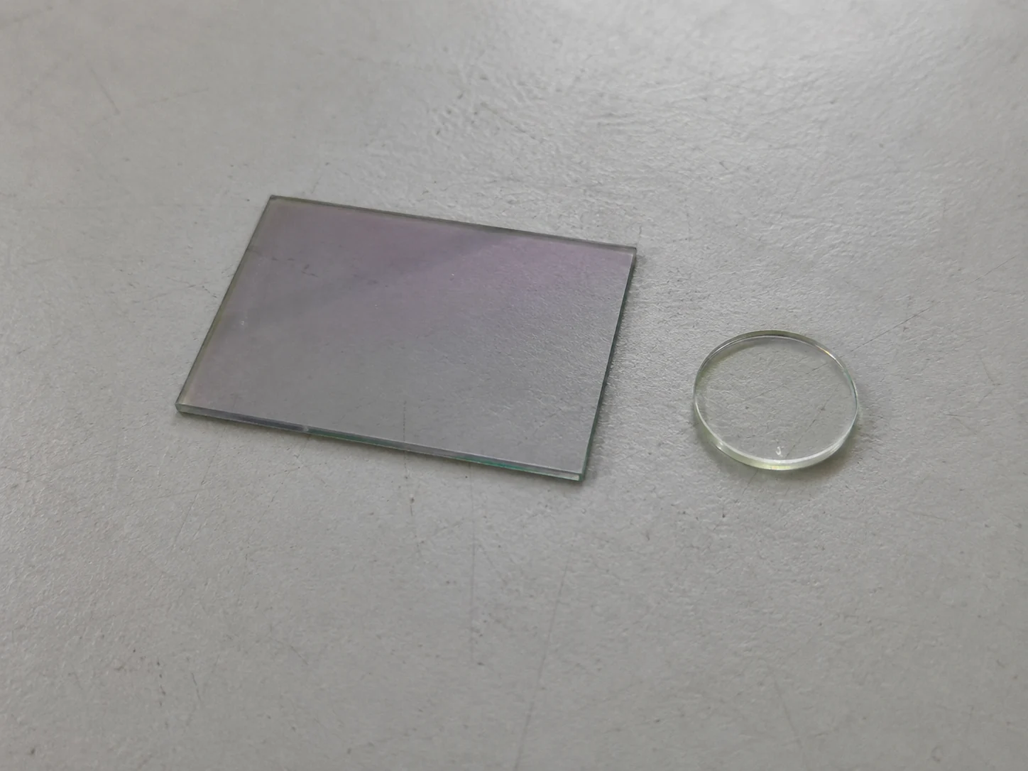
Alternating layers, interfaces and hybrid architectures that combine hardness, friction, barrier, optical or electrical functions within one coating system.
Material examples indicate NTI’s technology and development space. Final coating chemistry, thickness and process route are qualified against the substrate, geometry, performance target and production requirement.
NTI coating technologies extend functional thin films across metals, glass, ceramics, polymers, elastomers and semiconductor materials, creating more freedom to improve surface performance while retaining the substrate selected for the product.
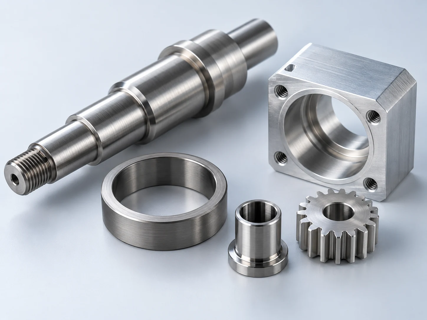
Steel, stainless steel, aluminium, titanium, copper and selected engineering alloys.
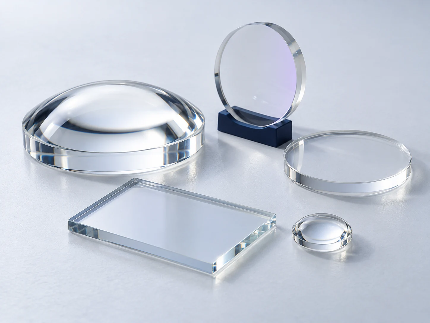
Optical glass, quartz and selected specialised glass materials for optical and functional surfaces.
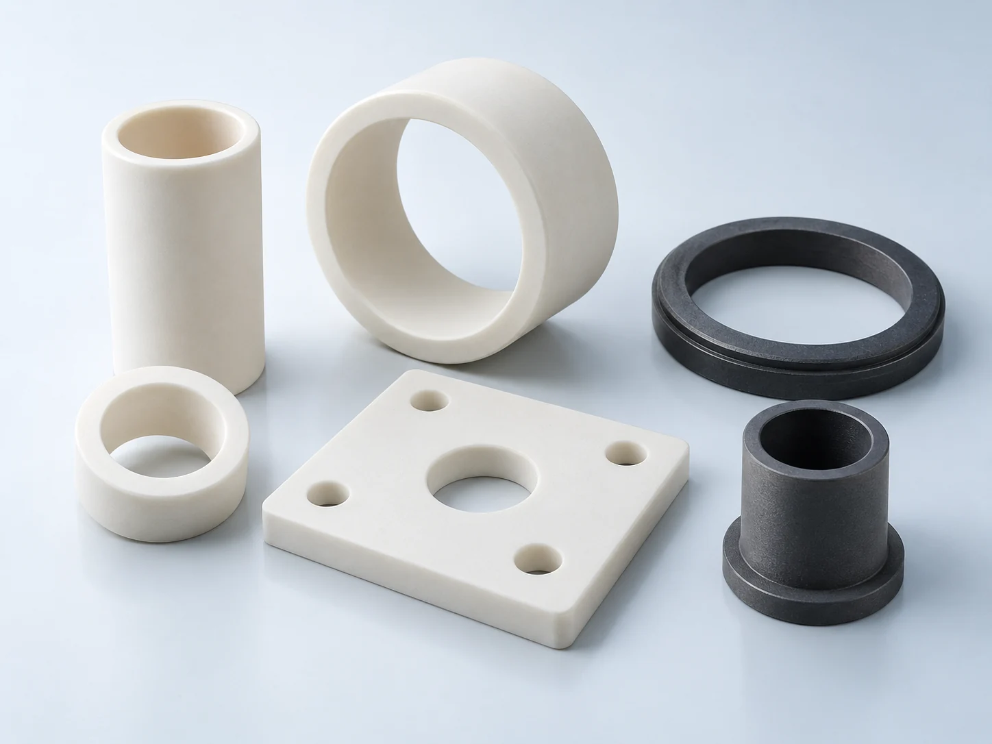
Engineering ceramics and selected functional ceramic components requiring wear, release, optical or barrier functions.
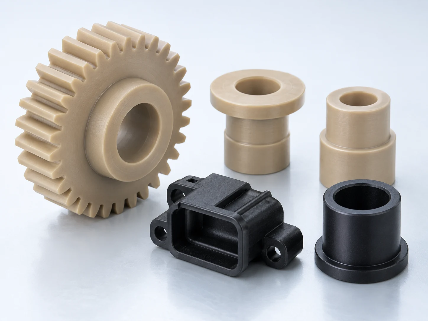
Selected engineering polymers where thermal tolerance, outgassing and interface design are compatible with the process.
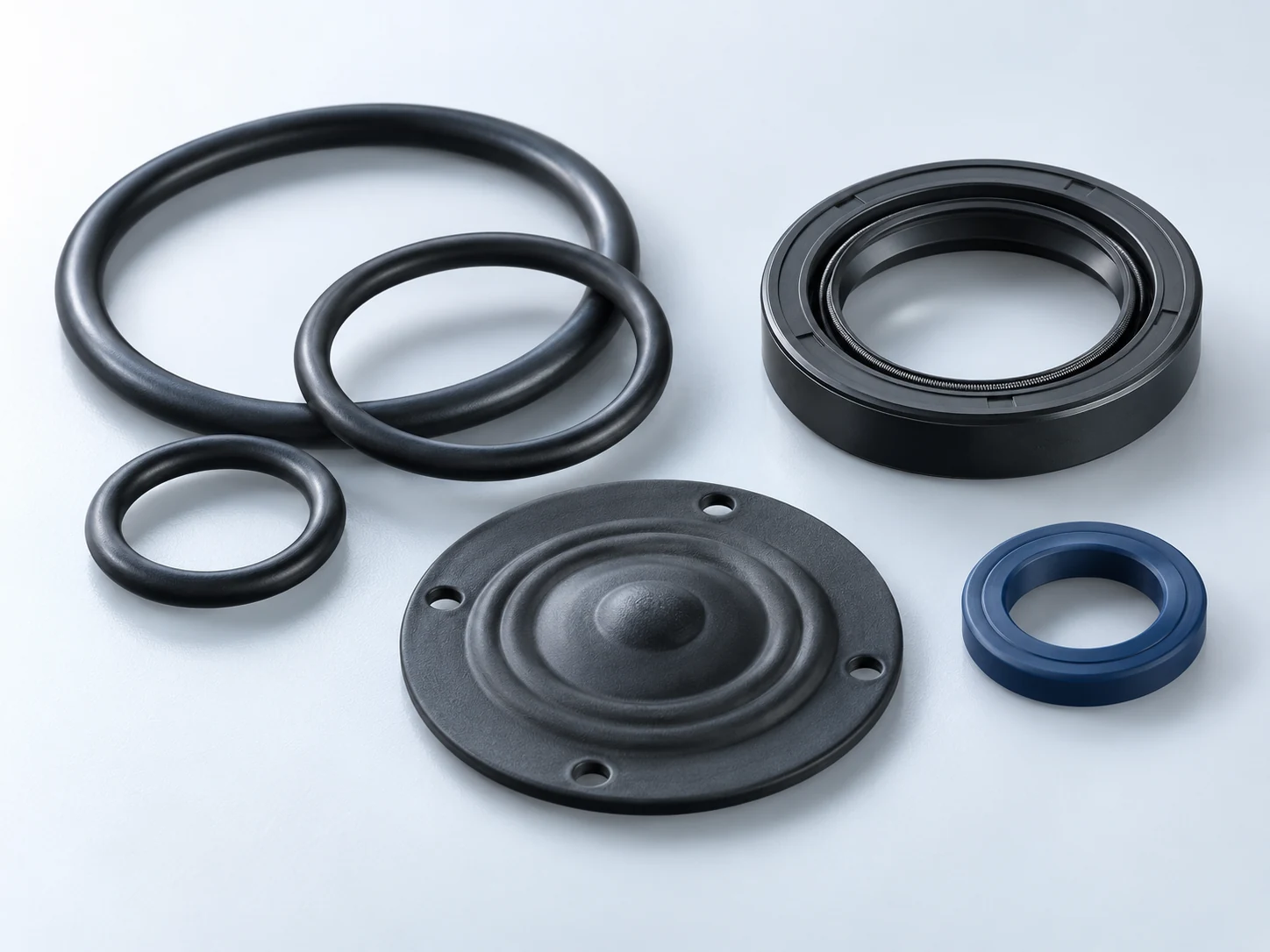
Selected flexible substrates for specialised low temperature surface functions and qualified coating architectures.
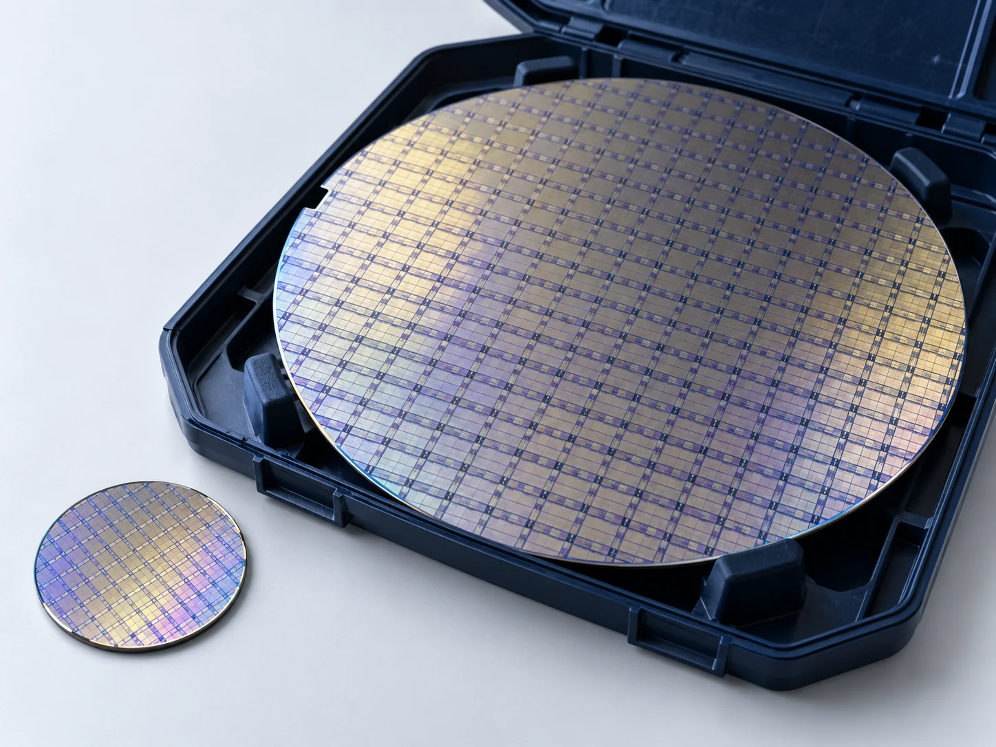
Silicon and selected materials used across semiconductor, microtechnology and precision device manufacturing.
Final coating compatibility depends on substrate composition, thermal tolerance, vacuum outgassing, geometry, surface condition, pretreatment and the required film architecture.
From ultra hard ta-C and hydrogenated DLC to dense hard coatings, precision optical films and multilayers, NTI combines five deposition technologies to address a wider range of surface performance requirements.
Filtered Highly Ionised Plasma for Dense, Smoother Thin Films
FCVA is an advanced cathodic arc PVD process. Localised cathode spots convert a solid source into highly ionised plasma, while a curved magnetic filter guides charged film forming species toward the substrate and substantially reduces the transfer of arc generated droplets and macroparticles.
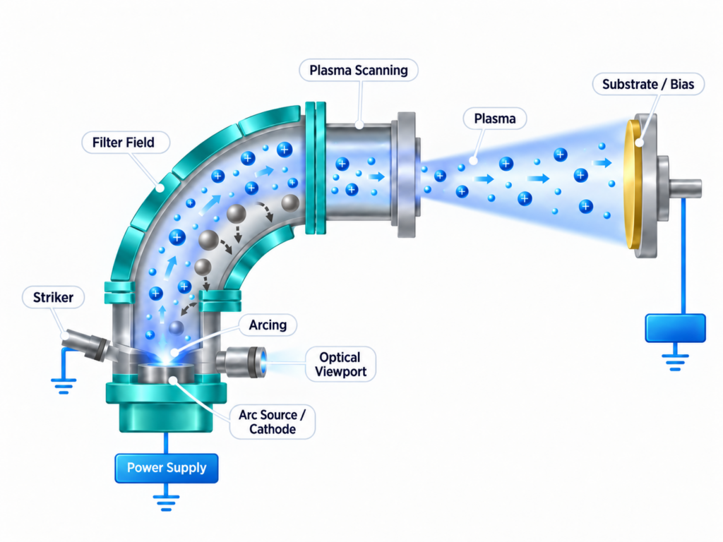
Localised cathode spots transform source material into an intense plasma containing energetic film forming ions.
Charged plasma follows the curved magnetic field while droplets and macroparticles are transported far less efficiently through the bend.
The filtered flux reaching the deposition zone is dominated by charged plasma rather than the neutral vapour typical of many conventional sputtering processes.
Bias and source conditions tune how ions interact with the growing surface, influencing density, stress, interface strength and carbon bonding.
For carbon, the correct ion energy window supports hydrogen free ta-C with high sp³ bonding potential and very high hardness.
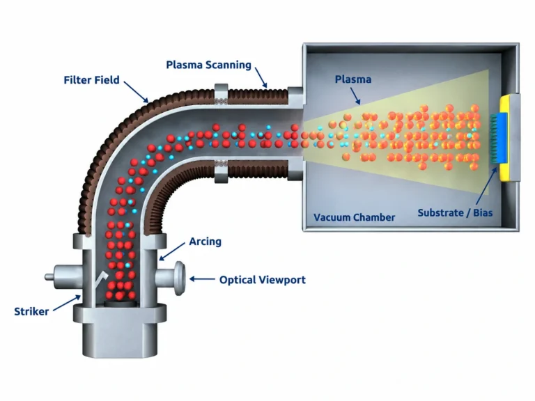
The curved magnetic filter steers charged plasma while droplets and macroparticles travel far less efficiently through the bend, reducing particle transfer and surface defects.
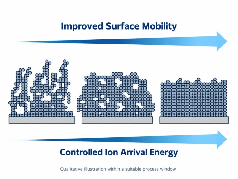
The high ion fraction allows substrate bias to control ion arrival energy, promoting dense film growth, interface mixing and strong adhesion without relying primarily on bulk substrate heating.
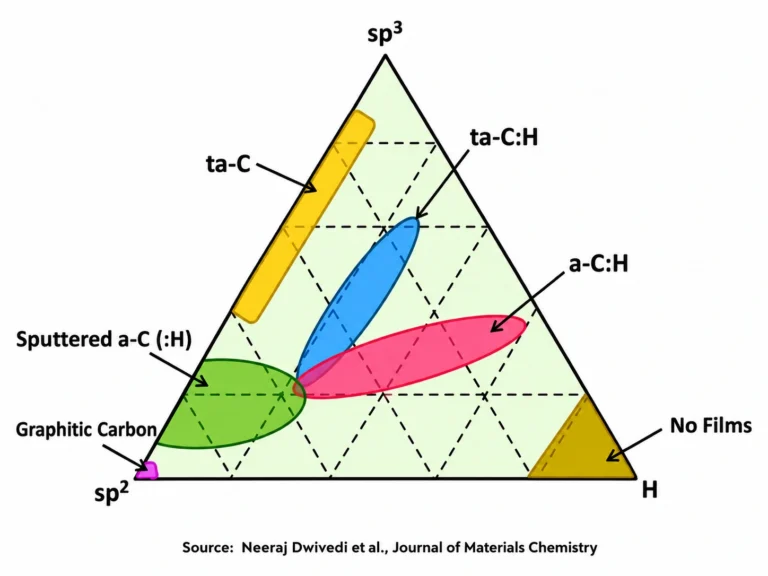
Carbon ion energy can be tuned into the ta-C growth window, supporting high sp³ bonding, very high hardness, low friction and exceptionally low wear.
Plasma Activated Carbon Chemistry for Low Friction DLC
PECVD introduces gaseous carbon precursors into vacuum and uses plasma energy to fragment and ionise them into reactive species. Those species react at the component surface to form hydrogenated DLC and related carbon films, with gas chemistry, power, pressure and bias controlling the deposition process.
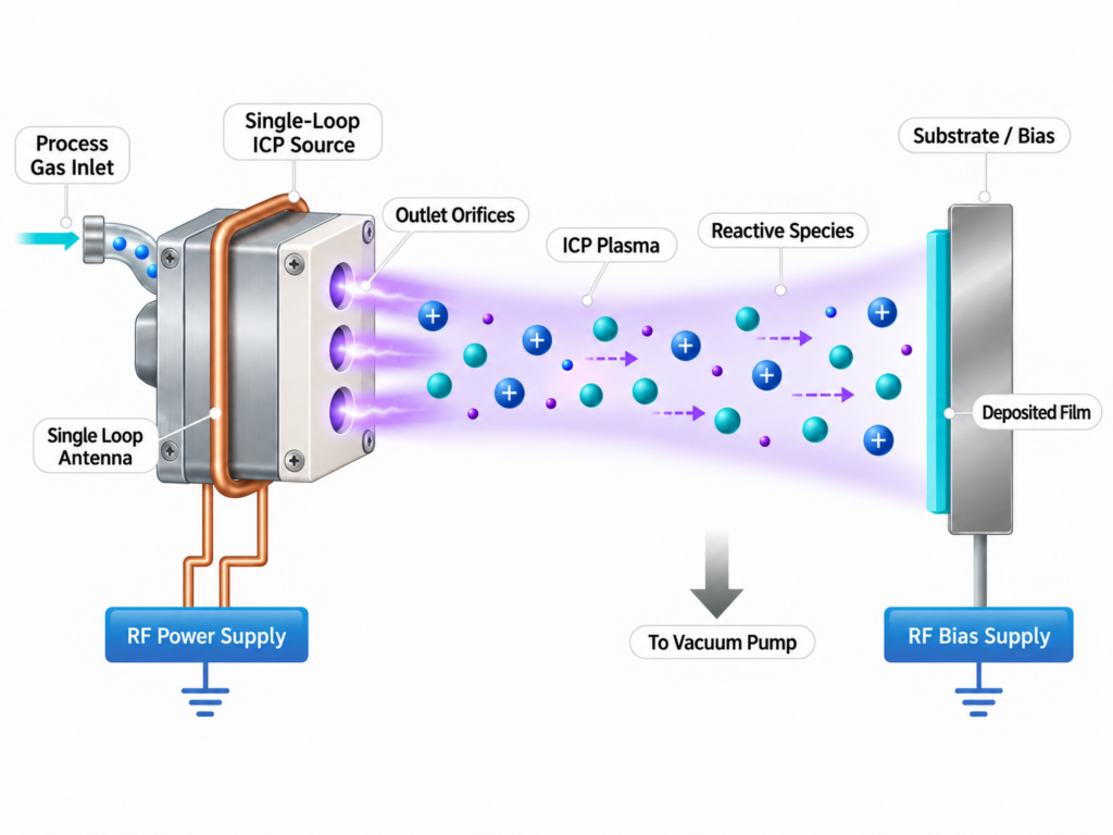
Hydrocarbon and selected functional precursors supply the elements that will form the coating.
RF, ICP or related plasma excitation fragments the precursor into reactive radicals and ions.
Plasma species are transported through the chamber and interact with the biased or grounded substrate.
Ion bombardment, pressure and power influence adhesion, density, stress and carbon structure.
Hydrogenated a-C:H and selected doped or functional carbon architectures form at substantially lower temperature than conventional thermal CVD.
Plasma dissociates hydrocarbon precursor gases and supplies reaction energy electrically, enabling a-C:H film formation at substantially lower temperature than conventional thermal CVD.
Precursor composition, plasma power and substrate bias adjust hydrogen content and carbon bonding, allowing hardness, friction, wear and residual stress to be balanced for the application.
Changing precursor chemistry and adding selected dopants can tune conductivity, corrosion resistance and wettability alongside the tribological response of the carbon film.
Highly Ionised Metal Plasma for Dense, Productive Hard Coatings
Cathodic Arc Evaporation creates localised arc spots on a solid metal cathode, generating a highly ionised metal plasma. The plasma travels directly toward the biased component and can react with gases such as nitrogen to form hard nitride and related compound coatings.
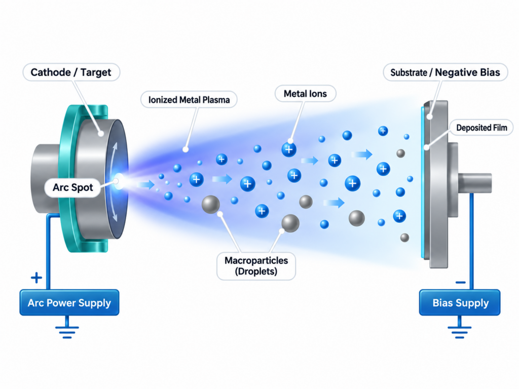
Mobile arc spots concentrate current into microscopic regions on the cathode surface.
The arc produces an intense metal plasma with much higher ionisation than conventional DC magnetron sputtering.
Arc processes can eject macroparticles; direct arc, multi arc, steered or column source strategies influence surface finish and productivity.
Metal ions react with gases such as nitrogen while substrate bias helps control bombardment and film density.
High ionisation and strong metal flux support robust nitride and related hard coating systems for demanding wear environments.
The large ion fraction can be accelerated by substrate bias, increasing interface energy and supporting dense microstructures with strong coating adhesion.
Cathodic arc ions arrive with significant kinetic energy, increasing surface mobility during film growth and supporting compact hard coatings for demanding contact conditions.
Metal cathodes combined with reactive gases enable hard nitride and carbonitride systems, while carbon cathodes provide a route to hydrogen free amorphous carbon coatings.
Directed Ion Beam Sputtering for Precision, Low Defect Thin Films
Ion Beam Sputtering directs a controlled beam of energetic ions onto a solid coating target. Momentum transfer ejects target atoms, which travel through high vacuum and condense on the substrate, separating material generation from the component and enabling precise control over beam energy and target sputtering.
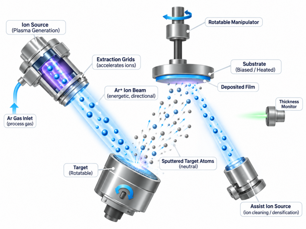
Energetic ions are extracted and directed toward the coating target with controlled beam conditions.
The beam transfers momentum to target atoms and ejects them by physical sputtering.
The coating material leaves the target as a controlled flux of sputtered atoms.
Low process pressure limits gas phase collisions so the sputtered material reaches the substrate under controlled transport conditions.
Controlled target sputtering supports smooth, dense and compositionally stable films for precision applications.
A controlled ion beam sputters the target in a defined geometry, supporting extremely smooth layers and low defect density for precision surfaces and optical film stacks.
Ion energy and beam current are controlled independently of the substrate, allowing target bombardment and film growth conditions to be tuned without sustaining a plasma around the component.
Reactive gases can be combined with ion beam target sputtering to form dense compound layers and nanometre multilayers for optical, barrier and other precision functional coatings.
Controlled Sputtering for Smooth, Compositionally Engineered Films
Magnetron Sputtering uses process gas ions to bombard a solid target while magnetic fields confine electrons close to the target surface. The resulting dense local plasma improves sputtering efficiency, while power mode, target selection and reactive gases control film chemistry and multilayer design.
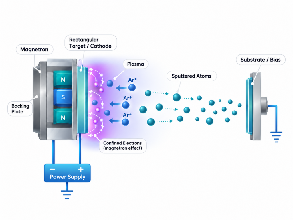
A solid target contains the material that will be transferred into the coating.
Electron trapping increases ionising collisions and sustains a dense plasma close to the target surface.
Energetic argon ions knock atoms from the target, creating a controlled material flux toward the component.
DC, RF, dual, cylindrical and pulsed modes, combined with reactive gases, expand target and coating options.
Controlled sputtering supports metallic, nitride, oxide and multilayer films with strong thickness and composition control.
Magnetic fields retain electrons close to the target, increasing plasma density and ionisation efficiency so sputtering can be sustained with stable, controlled material flux.
Target atoms are released by ion bombardment rather than cathode spot melting, avoiding the arc droplet mechanism and supporting smooth precision thin films.
Target selection, DC, RF or pulsed power and reactive gas control provide broad control over composition, stoichiometry, thickness and layer sequence.
Compare measurable performance windows across five vacuum deposition technologies, Type III Hard Anodizing and Hard Chrome Electroplating, including hardness, wear, friction, process temperature, service temperature and substrate compatibility.
| Characteristic | Filtered Cathodic Vacuum Arc | PECVD DLC | Cathodic Arc Evaporation | Ion Beam Sputtering | Magnetron Sputtering | Type III Hard Anodizing | Hard Chrome Electroplating |
|---|---|---|---|---|---|---|---|
| Deposition Process | Filtered cathodic arc PVD | Plasma enhanced CVD | Cathodic arc PVD | Ion beam sputter PVD | Magnetron sputter PVD | Electrochemical oxidation | Electrochemical metal deposition |
| Adhesion | Excellent | Very Good | Excellent | Very Good to Excellent | Good to Very Good | Integral oxide layer | Very Good |
| sp³ Content for Carbon Film Variants | Up to 88% | ~20 to 50% | ~40 to 70% | ~20 to 60% | ~20 to 55% | 0% | 0% |
| Hardness | Up to 5,500 HV | ~1,500 to 4,000 HV | ~1,800 to 3,800 HV | Up to ~4,000 HV | ~1,000 to 3,000 HV | ~400 to 600 HV | ~850 to 1,050 HV |
| Wear / Abrasion | <1 × 10⁻⁸ mm³/N·m | ~10⁻⁸ to 10⁻⁷ mm³/N·m | ~10⁻⁷ to 10⁻⁵ mm³/N·m | ~4 × 10⁻⁷ mm³/N·m | ~10⁻⁷ to 10⁻⁶ mm³/N·m | ≤1.5 mg / 1,000 cycles Taber | ~2 to 3 mg / 1,000 cycles Taber |
| Friction Coefficient | ~0.1 | ~0.1 to 0.2 | ~0.06 to 0.6 | ~0.08 to 0.10 | ~0.1 to 0.6 | ~0.4 to 0.5 | ~0.16 to 0.21 |
| Process Temperature | <80°C | ~160 to 250°C | ~150 to 550°C | Room temperature to ~200°C | ~150 to 500°C | ~−4 to 4°C bath | ~50 to 60°C bath |
| Maximum Service Temperature | Up to 600°C | ~300 to 350°C | Up to ~1,100°C | ~400°C | Up to ~700°C | ~200°C continuous | Up to ~425°C |
| Compatible Substrate | Metals, alloys, ceramics, glass, selected polymers and elastomers | Metals, alloys, ceramics, glass and selected polymers | Metals, alloys, tools and selected ceramics | Glass, optical materials, metals, ceramics and semiconductors | Metals, alloys, glass, ceramics, semiconductors and selected polymers | Aluminium and aluminium alloys | Steels, stainless steels, cast iron, copper alloys and selected conductive metals |
Values shown are published industrial ranges and NTI process data for preliminary technology comparison. Performance varies with coating chemistry, thickness, substrate, pretreatment, test method and operating environment. sp³ values apply to carbon film variants. Wear and abrasion values use the established test metric commonly reported for each surface treatment and are not directly interchangeable across methods. Final specifications are confirmed during application qualification.
NTI thin film platforms translate into surface functions that extend component life, reduce friction, improve release, control electrical and optical behaviour, enhance appearance and protect critical interfaces.
Reduce wear, lower friction and protect high duty surfaces under repeated mechanical contact.
Reduce adhesion, residue and release force on molds, forming surfaces and production interfaces.
Engineer conductivity, ESD, electrical insulation and contact behaviour at the surface.
Control reflection, transmission, filtering and optical response for lenses, displays, sensors and precision optics.
Bring colour, metallic character and premium appearance together with production durability.
Lower surface energy to repel water and oils, reduce smudging and support easier cleaning on qualified surfaces.
Engineer wear, friction, visibility, corrosion and barrier functions for qualified medical applications.
Balance corrosion protection, conductivity and durability for metallic bipolar plates and selected energy interfaces.
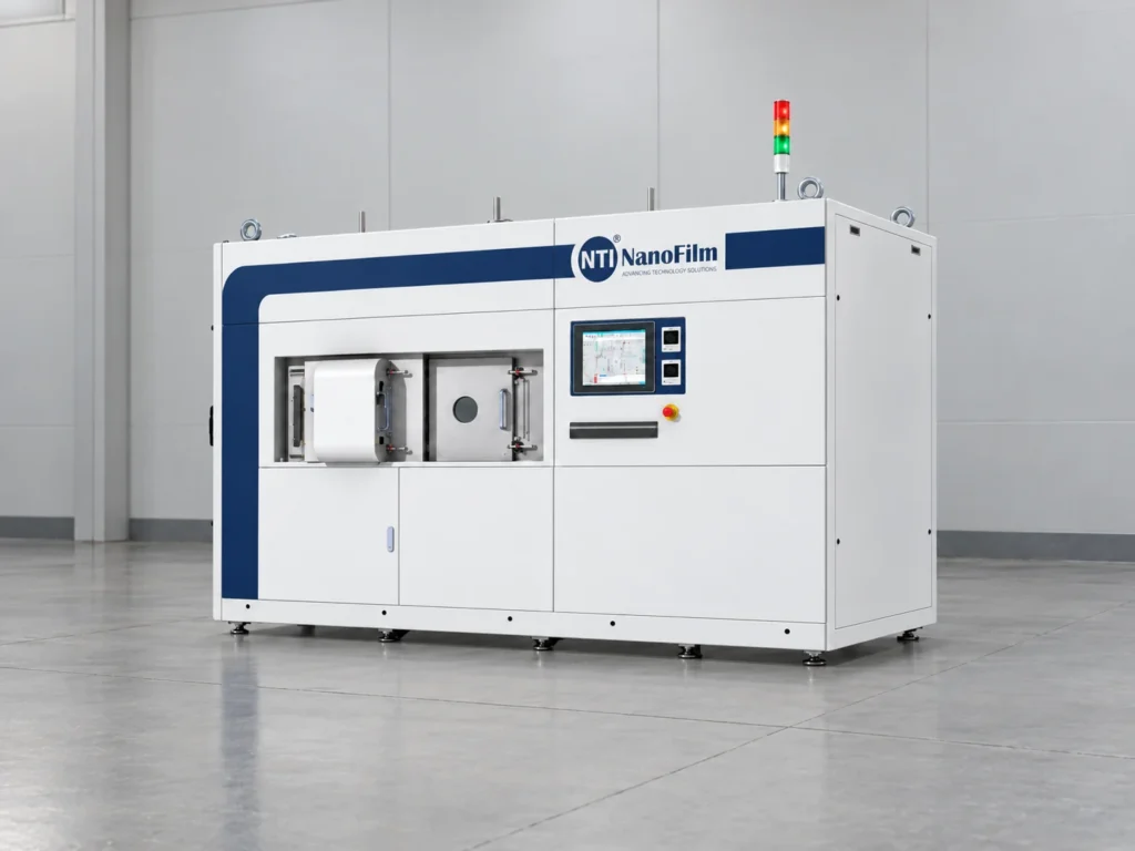
With 27+ years of coating and production experience, NTI has developed coating processes, proven them in production and engineered the equipment that industrialises them. Explore platforms designed around different throughput, handling and coating requirements.

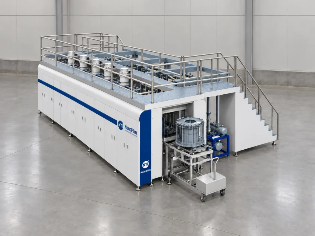
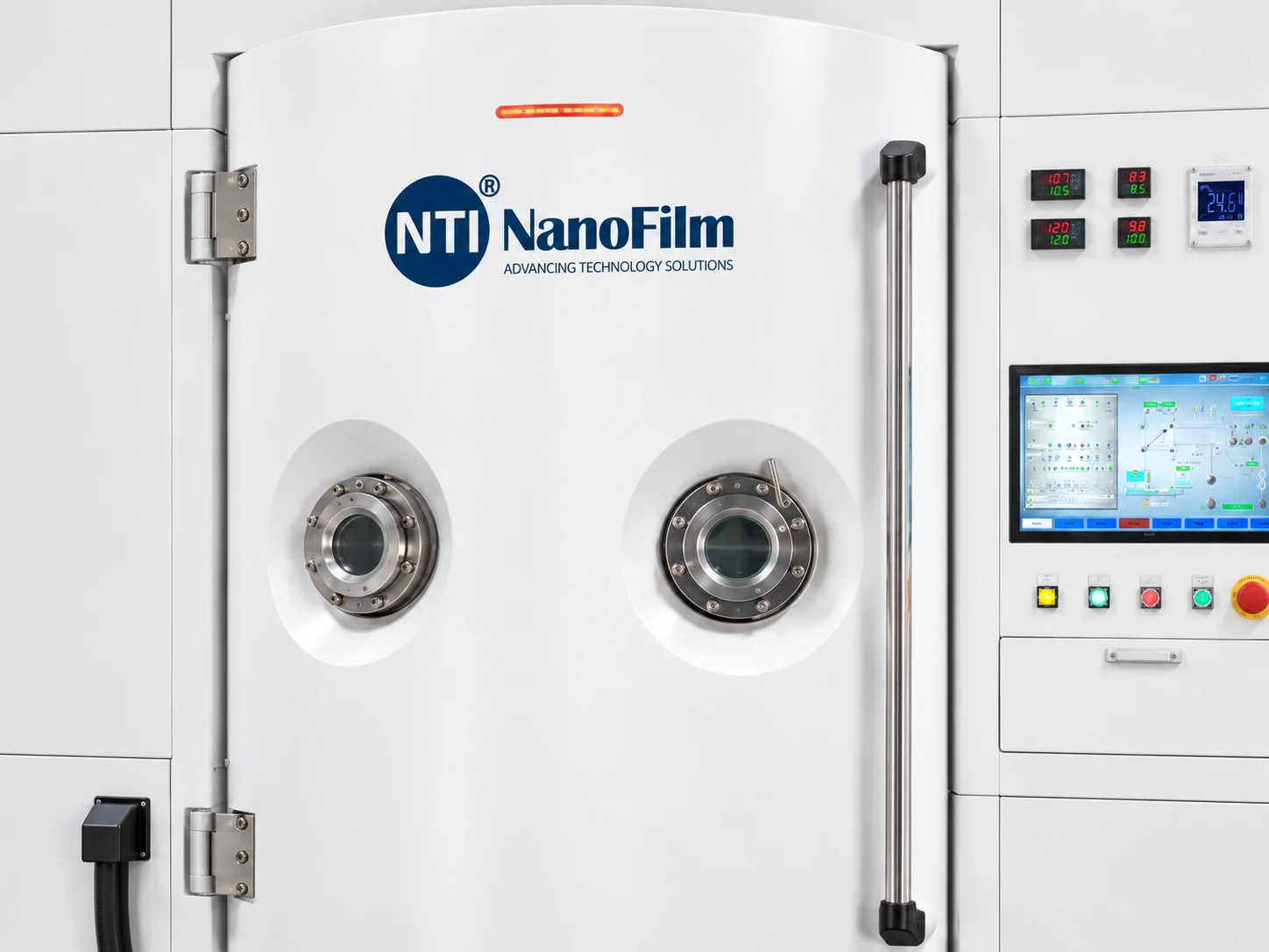
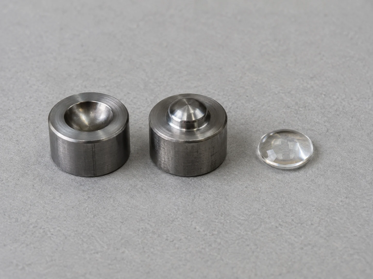
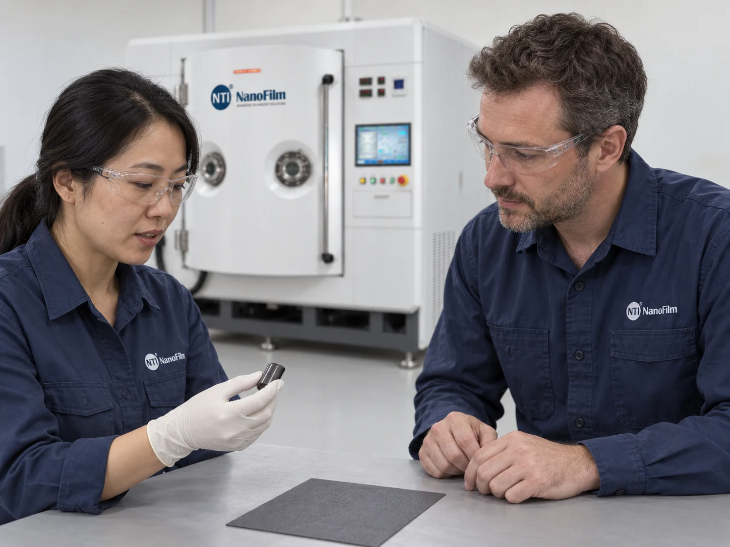
Bring us the component, substrate and performance target. NTI Nanofilm can help define the coating material, select the deposition technology, prove the process and build the path toward industrial production.
Physical Vapor Deposition, or PVD, is a family of vacuum coating processes that forms thin films from a solid target or cathode. Material is released by sputtering or cathodic arc plasma, transported through vacuum and condensed on the component. NTI PVD technologies include Filtered Cathodic Vacuum Arc, Cathodic Arc Evaporation, Ion Beam Sputtering and Magnetron Sputtering.
Plasma Enhanced Chemical Vapor Deposition, or PECVD, forms a film from gaseous precursors activated by plasma. PVD starts from a solid material source and transfers that material physically, while PECVD uses plasma driven chemistry at the surface. PECVD is especially useful for hydrogenated DLC and other functional films that benefit from lower process temperatures than conventional thermal CVD.
FCVA is a cathodic arc PVD process that guides highly ionised plasma through a curved magnetic filter before deposition. The filter substantially reduces arc generated droplets and macroparticles while retaining an ion rich deposition flux. For carbon coatings, NTI FCVA can produce hydrogen free ta-C with sp³ content up to 88%, hardness up to 5,500 HV and a friction coefficient around 0.1.
Both technologies generate highly ionised cathodic arc plasma. Conventional Cathodic Arc Evaporation sends the plasma more directly toward the substrate and is widely used for dense hard coatings such as nitrides. FCVA adds magnetic plasma filtration to reduce macroparticle transfer before the plasma reaches the component, making it particularly valuable where smoother precision surfaces and high sp³ ta-C are required.
Magnetron Sputtering is a PVD process in which magnetic fields confine electrons near a solid target, increasing plasma density and sputtering efficiency. Target selection, power mode and reactive gases enable metals, alloys, nitrides, oxides, carbides and multilayer thin films for optical, electrical, decorative, barrier and tribological applications.
Ion Beam Sputtering uses a dedicated ion source to direct energetic ions onto a solid target. Sputtered target atoms then form the thin film on the substrate. The process is used when very smooth, low defect and tightly controlled films are important, including precision optical layers, nanometre multilayers, dielectric coatings and selected DLC systems.
DLC is a broad family of amorphous carbon coatings containing different proportions of sp² and sp³ carbon bonding and, in many cases, hydrogen. ta-C is a hydrogen free DLC with a high sp³ fraction. NTI FCVA ta-C can reach up to 88% sp³ bonding, giving a combination of very high hardness, low friction and strong wear resistance.
The best route depends on the substrate, load, temperature, lubrication and surface finish required. FCVA ta-C is a strong choice for very high hardness, low wear and friction around 0.1. PECVD DLC provides low friction with tunable hydrogenated carbon chemistry, while Cathodic Arc and Magnetron Sputtering support hard nitrides, carbonitrides and multilayers for different wear and temperature conditions.
PVD and PECVD can coat many metals and alloys, ceramics, glass and optical materials, semiconductor materials and selected polymers or elastomers. Final compatibility depends on substrate composition, thermal tolerance, vacuum outgassing, geometry, surface condition, pretreatment and the required coating architecture.
Process temperature varies by deposition technology and coating chemistry. Selected NTI FCVA processes can operate below 80°C, PECVD DLC is commonly below about 250°C, and industrial sputtering or cathodic arc hard coating processes can extend from low temperature variants into several hundred degrees Celsius. The final process window is selected around the substrate and coating requirement.
PVD and PECVD are dry vacuum deposition processes and do not require the aqueous anodizing or electroplating bath used during wet surface treatment. They create thin functional films across carbon, metals, nitrides, oxides and multilayers. Type III hard anodizing forms an integral oxide mainly on aluminium, while hard chrome electroplating deposits chromium from a liquid electrolyte onto conductive substrates.
Selection starts with the required surface function and operating conditions. FCVA is strongest for filtered highly ionised deposition and high sp³ ta-C; PECVD DLC for tunable hydrogenated carbon chemistry; Cathodic Arc for dense adherent hard coatings; Ion Beam Sputtering for ultra smooth precision films; and Magnetron Sputtering for broad material, composition and multilayer control. Substrate, geometry, temperature limit, thickness and production volume then determine the final process.