As smartphones become more refined, consumers expect the flash area to blend seamlessly into the device while still delivering clearer, more natural-looking images in low-light conditions.
Visible LEDs, internal structures and concentrated hotspots can undermine both the appearance of the phone and the quality of the photography experience.
For brand owners and manufacturers, meeting these expectations requires more than optical performance alone. The flash lens must also withstand downstream assembly without yellowing or degrading, as limited reflow resistance can lead to cosmetic defects, inconsistent performance and potential yield loss during production.
The Product and Manufacturing Challenge
The conventional smartphone flash-lens approach created three connected limitations driven by consumer expectations and production needs.
Visible internal structure
The LED and internal components remained visible through the lens, affecting the perceived cleanliness of the flash area.
Flash hotspot in low light
Concentrated light output could still create visible hotspots in smartphone flash photography.
Yield risk during assembly
The injection-molded lens showed yellowing risk at higher temperature, creating potential cosmetic and production-yield concerns.
One lens, multiple expectations
The flash lens needed to support appearance, optical performance and downstream thermal reliability together.
The NanoFab Contribution
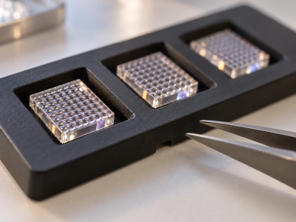
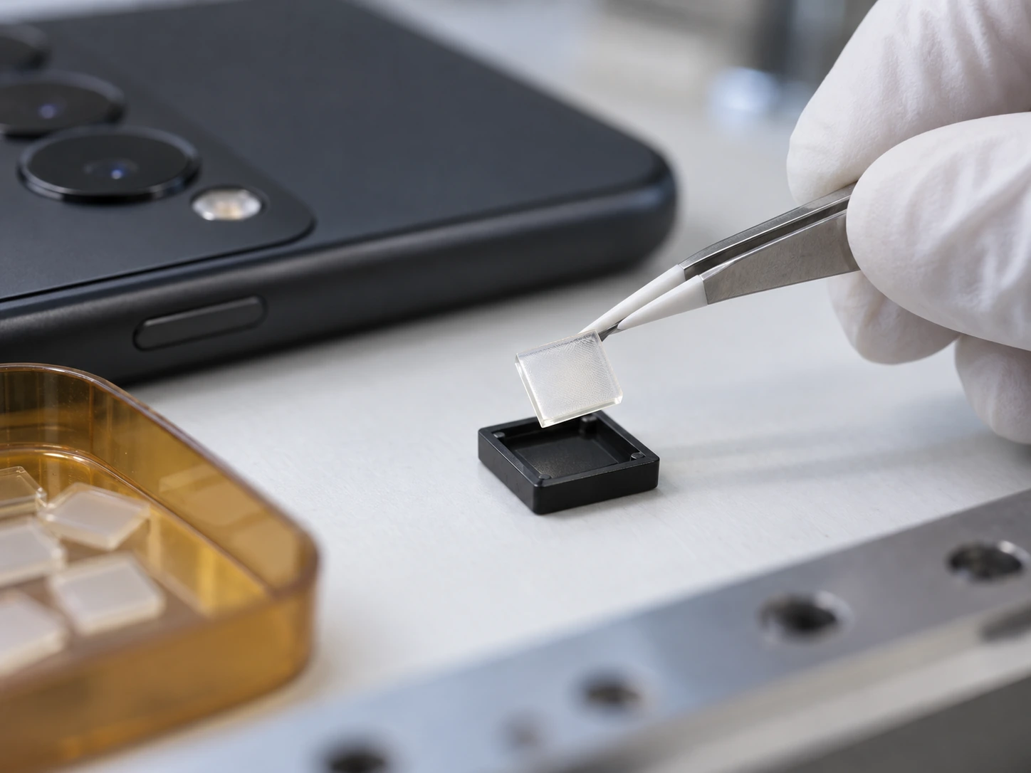
NanoFab developed a replicated polymer micro-optic combining prism Fresnel and microlens-array features in UV-cured epoxy.
The microstructured surface redistributed the LED output while reducing the visibility of internal components. The replication route also supported a material and process path suited to higher-temperature downstream assembly.
Micro-optics design-to-manufacturing approach
The solution was developed to connect product appearance, optical uniformity and assembly reliability into one component design.
- Prism Fresnel featuresSupport light redirection and compact optical control.
- Microlens-array structuresHelp improve light distribution and concealment.
- UV-cured epoxy replicationTransfers the microstructured surface repeatably.
- Reflow-ready designSupports downstream assembly at elevated temperature.
Solution and Performance Outcome
NanoFab redesigned the flash lens using prism Fresnel and microlens-array structures in a UV-cured replicated optic. The new design improved internal-component concealment, reduced flash hotspots and supported five reflow cycles at 260°C, helping address both user experience and production yield concerns without treating each issue as a separate design problem.
Cleaner flash-window appearance
Prism Fresnel and microlens-array structures reduced the visibility of the LED and internal components.
More uniform low-light illumination
The microstructured surface redistributed LED output to reduce concentrated hotspots.
Reflow-ready replicated optics
UV-cured epoxy replication supported five reflow cycles at 260°C.
Production-ready component path
The process supported high-volume replicated polymer optics for compact consumer devices.
The replicated flash lens maintained the required thermal-performance target at 260°C.



Business Impact
The solution combined aesthetic improvement, optical performance and thermal robustness in one component. This addressed concealment, light uniformity and reflow resistance together rather than as separate design problems.
For smartphone and compact-device programmes, the same design-to-manufacturing approach can support differentiated appearance and high-volume replicated polymer optics.