Material selection has become a defining part of premium smartphone design.
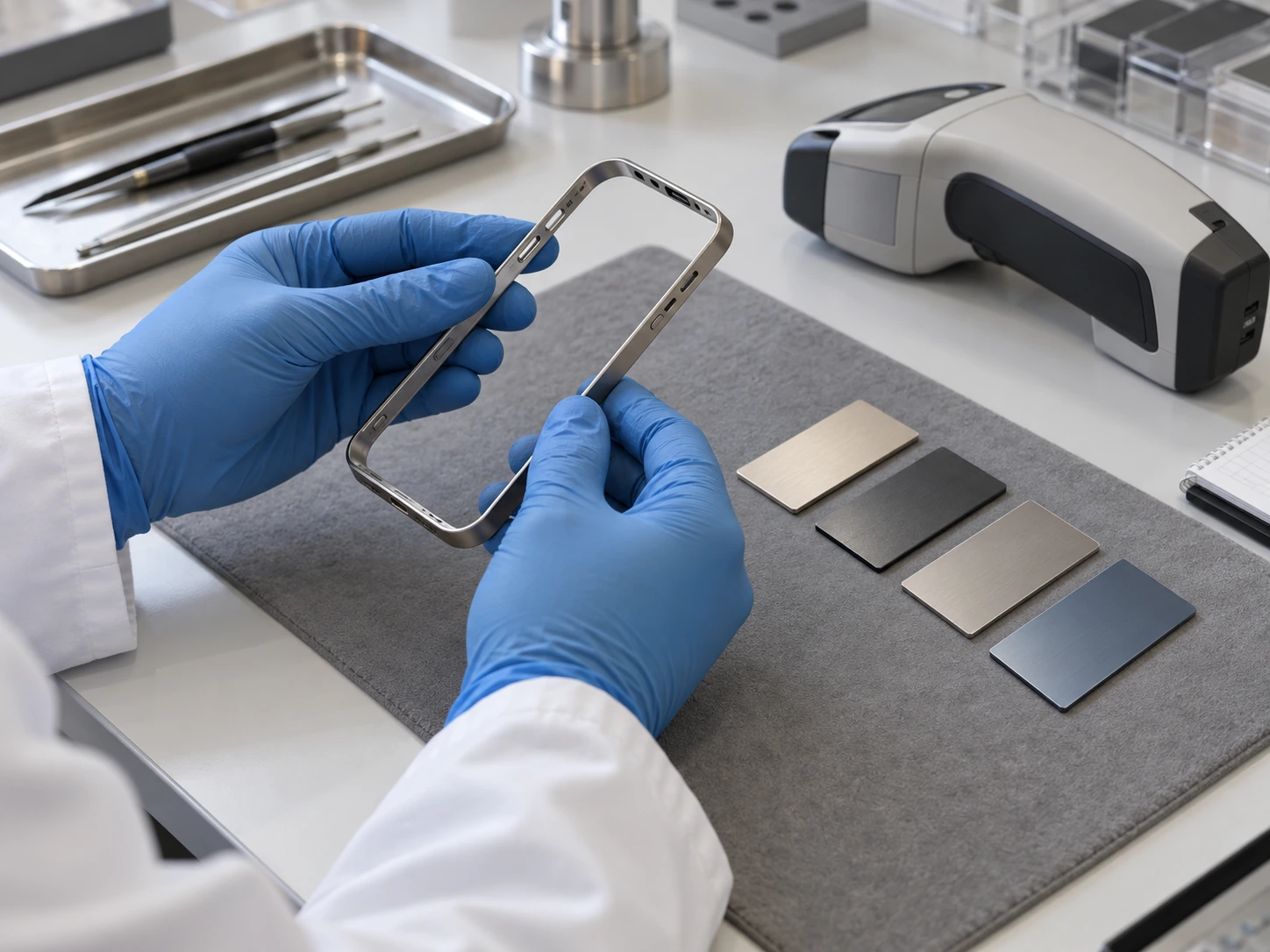
Across successive product generations, device makers have moved between stainless steel, aluminium alloys and titanium to balance strength, weight, thermal performance and product distinction. Titanium introduced a compelling combination of structural strength, lower weight and premium material character, creating new possibilities for flagship device design.
However, adopting a new enclosure material also changes the manufacturing requirements behind the product.
The coating must bond reliably to the substrate, preserve the intended metallic character and remain visually consistent across complex geometries and large production volumes. The commercial value of the material shift would ultimately depend on whether the new surface could be qualified, reproduced and scaled without compromising appearance, durability or production efficiency.
The Manufacturing Challenge
A titanium finish that met the design intent at prototype stage still had to perform consistently across production fixtures, chamber positions and manufacturing batches.
Small variations in surface preparation, coating thickness or deposition conditions could alter the colour, tone and reflectivity of the enclosure. On a premium device, these differences could become visible mismatches, increase inspection and rework, or reduce confidence during production qualification.
The challenge was therefore not simply to develop a decorative finish for titanium.
It was to establish a repeatable surface-engineering process capable of preserving the approved appearance while meeting the output, quality and reliability expectations of high-volume manufacturing.
The NTI Contribution
NTI Nanofilm developed a calibrated PVD sputtering process around the titanium substrate, enclosure geometry and finish requirements.
The work integrated surface preparation, coating-layer design, source calibration, custom fixturing and deposition control into one manufacturing process. Each parameter had to remain aligned so that coating adhesion, surface appearance and production repeatability could be maintained together.
Through calibration, variation across both chromium and silicon coating sources was brought below 10%.
| Coating Source | Variation Before Calibration | Variation After Calibration |
|---|---|---|
| Chromium | 40.94% | 9.51% |
| Silicon | 40.31% | 9.94% |
By bringing both coating sources into a tighter control window, NTI supported more consistent coating thickness, tone and reflectivity across the production area.
Deposition rates were tuned to maintain the appropriate film-growth window rather than maximise speed alone. This helped support smoother surface formation, controlled colour development and lower visible variation between coated components.
From Qualification to Volume Production
The process was supported by NTI’s in-house high-volume coating platform, combining component cleaning, fixture engineering, calibrated sputtering, process inspection and outgoing quality control.
The optimized platform strengthened production readiness by increasing batch capacity and shortening preparation time between batches, achieving:
Up to 1,440 components per batch, compared with the earlier 1,200-component baseline.
Reduced from 150 minutes to improve production readiness between batches.
These improvements brought together the two requirements that determine whether a new material can succeed commercially.
The calibrated coating process supported a more repeatable surface appearance, while the production platform increased batch capacity and shortened preparation time. Together, they helped move the titanium enclosure from surface qualification toward stable high-volume manufacturing.
Business Impact
The programme demonstrated how surface engineering can turn a material decision into a manufacturable product advantage.
By bringing both chromium and silicon coating variation below 10% and strengthening production capacity, NTI helped preserve the distinctive appearance of titanium while improving repeatability, throughput and manufacturing confidence.
For the device maker, this supported a differentiated material identity without compromising the production discipline required for a globally scaled consumer product.
The achievement was not simply the application of a new coating. It was the establishment of a controlled manufacturing route through which a new enclosure material could be introduced with greater confidence.
Enabling the Next Material Transition
Consumer-electronics material strategies will continue to evolve.
Titanium remains relevant where strength, thinness and premium character lead the design brief. Aluminium alloys are gaining renewed attention where thermal management, lower weight and production efficiency are priorities. Stainless steel, glass, ceramics, polymers and composite structures each introduce different requirements for adhesion, colour, durability and process temperature.
The material may change, but the commercial challenge remains consistent: its surface must be engineered to deliver the intended product experience repeatedly and at scale.
NTI Nanofilm supports device makers from material evaluation and coating development through process qualification and high-volume manufacturing, helping turn the next material transition into a production-ready product surface.