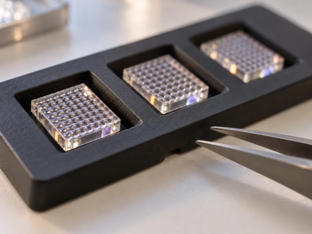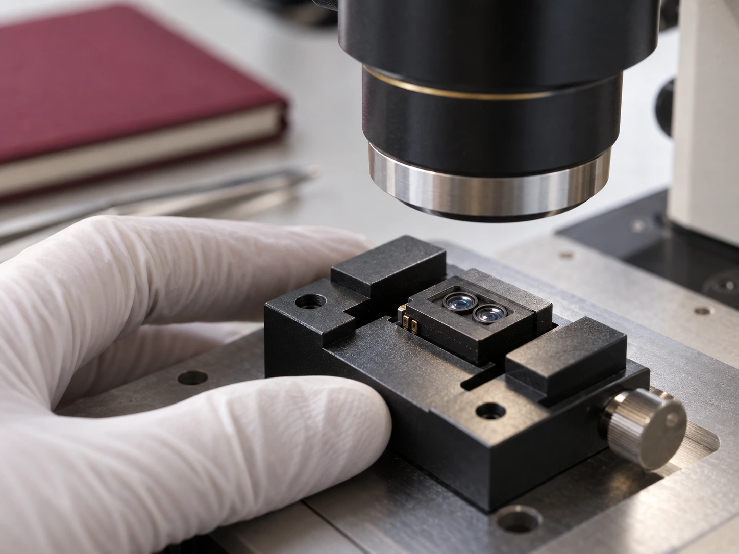
In smartwatch health-sensing modules, performance depends not only on the lens design, but also on how efficiently the lens can be integrated into the package and how closely the final profile matches the target geometry.
Multiple separate lenses can add downstream assembly steps, while lower lens-profile matching can limit the optical system’s ability to direct and collect light efficiently.
NanoFab therefore combined lens-in-package integration with accurate 5-axis SPDT mastering, proprietary CAM and controlled production to simplify assembly and bring the final lens profile closer to the target design.
Product and Manufacturing Challenge
The smartwatch module used multiple separate lenses that required additional assembly, while the final lens profile needed to match the intended design more closely to improve sensing performance.
Downstream assembly complexity
Most smartwatch sensing modules use at least two separate lenses, adding downstream assembly steps and increasing module-integration complexity.
Lens-profile matching
The previous production approach achieved about 70% match to the target design, limiting optical efficiency and sensing sensitivity.
NanoFab Solution Results
| NanoFab Solution | Commercial Result |
|---|---|
| Lens-in-Package Integration | Simplified Downstream Assembly |
| Lens-Profile Matching Improved from 70% to 95% | Improved Sensing Sensitivity and Reduced Power Consumption |
Benefit and Performance Outcome
The solution connected package integration with profile control, resulting in simpler assembly and improved sensing sensitivity with reduced power consumption.
Simplified downstream assembly
Integrating the lens directly into the package reduced loose-part handling and downstream assembly operations.
Improved sensing sensitivity
Better profile matching helped the optical system use emitted light more efficiently, reducing power consumption that helps to improve battery life.
Closer alignment to the target lens geometry supported stronger optical performance for health-sensing applications.





Product and Manufacturing Value
The solution addresses module integration and optical performance together. Lens-in-package integration simplifies downstream assembly, while controlled 5-axis SPDT mastering and our in-house process improve how closely the manufactured lens form matches the target geometry.
This supports simpler module builds, more reliable health-sensing performance and lower power consumption that can help improve battery life. For smartwatch and wearable-health programmes, the approach provides a more production-ready route that combines optical function and package integration in one component strategy.