
NTI Nanofilm combines FCVA ta-C, DLC and hard coating technologies with coating services, industrial coating equipment and application development to help protect uptime, protect yield and extend critical component life across semiconductor equipment surfaces.
AI demand, advanced nodes and advanced packaging are increasing equipment usage, process sensitivity and surface-related risk. Coatings help control wear, sticking, ESD, particles and burrs before they affect uptime, yield and production continuity.

Higher output means more equipment cycles, contact wear and cleaning stops. Coated surfaces help tools run longer and keep production flow stable.
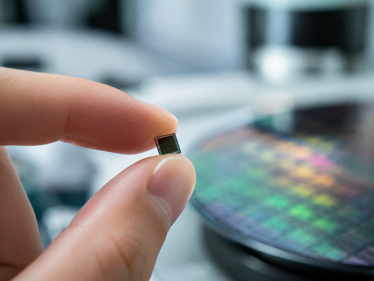
Smaller features and tighter margins leave less room for ESD, particles or surface drift. Stable coated surfaces help protect yield-sensitive steps.
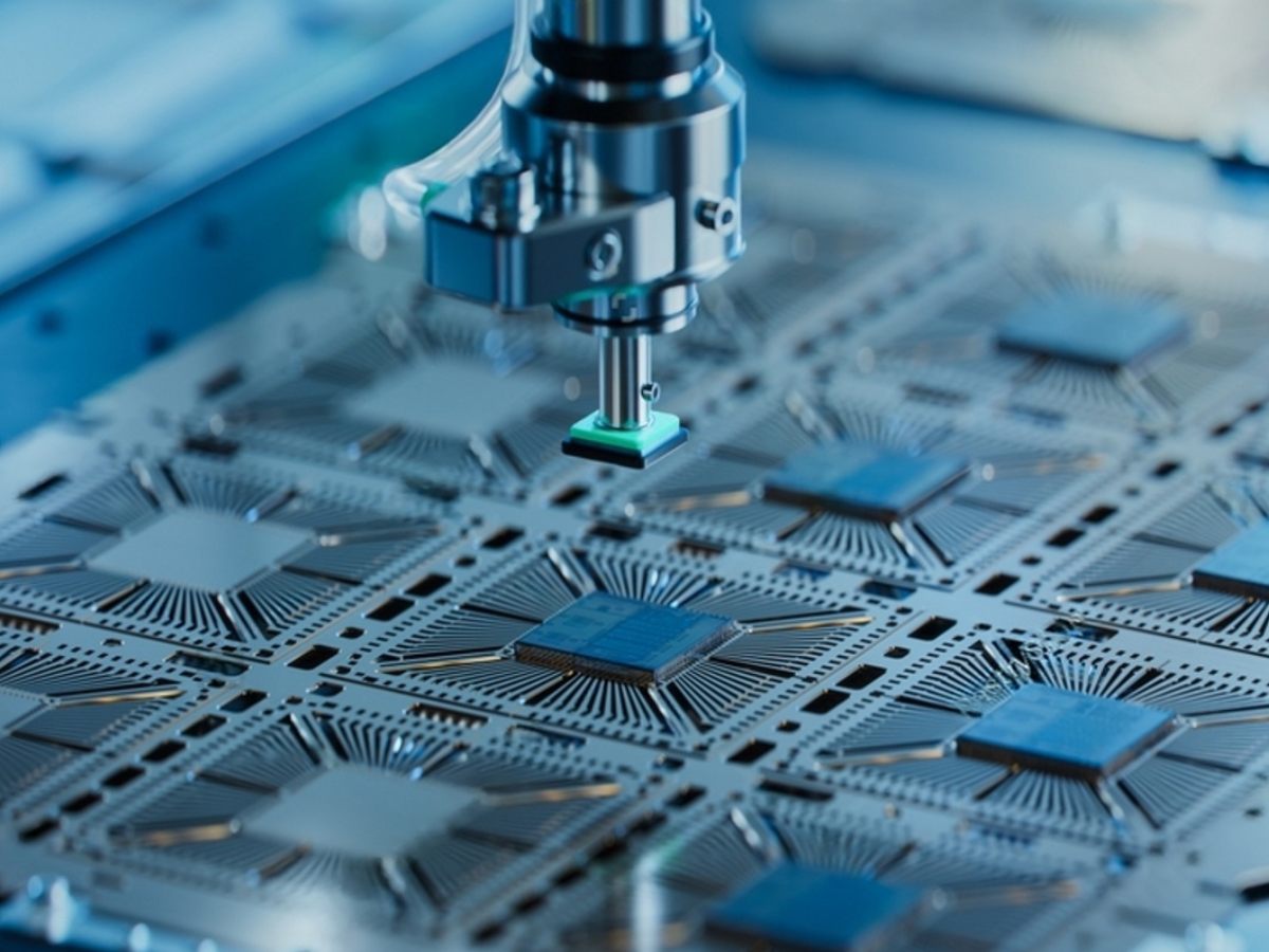
Chiplets, HBM and 2.5D/3D packaging add more value near final assembly. Coatings help reduce wear, sticking and contamination risk.

Longer tool life and fewer service stops reduce replacement pressure, scrap and delivery risk. Stable coating pathways help support resilient production planning.
Select the requirement closest to your application to see how working-surface condition can influence tool life, release behaviour, charge control, particle generation, edge quality and process stability, together with the NTI portfolio most relevant to that need.
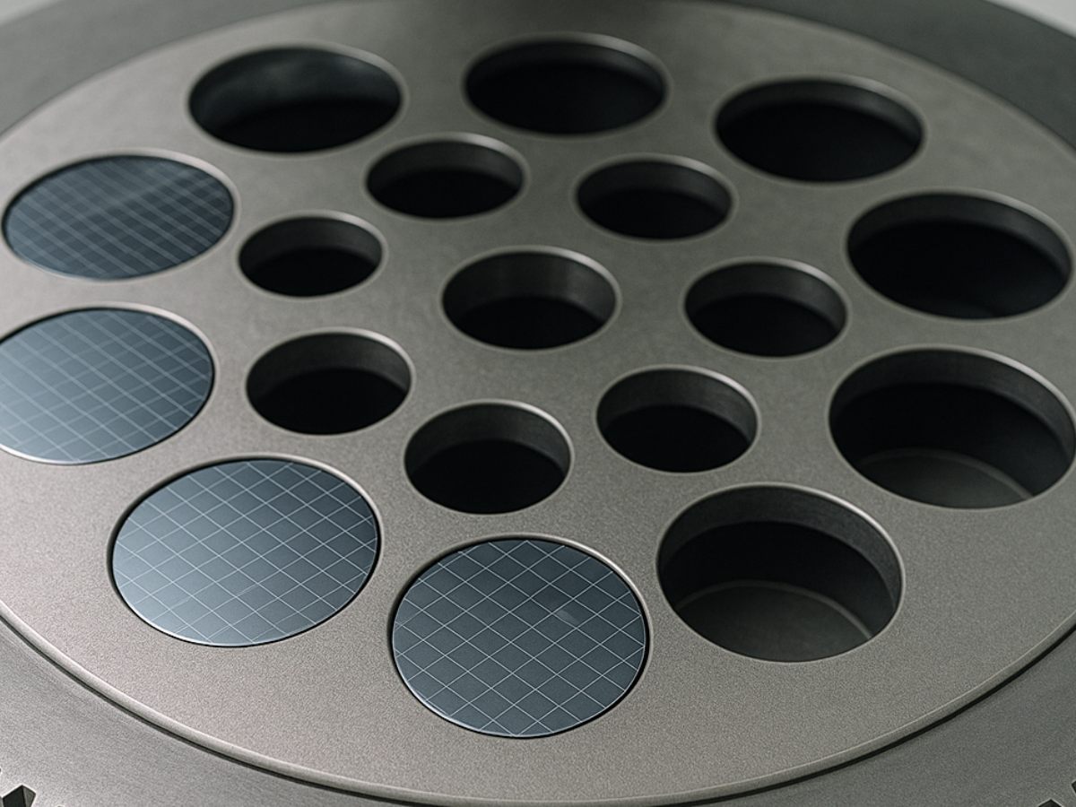
Repeated contact across lapping carriers, capillaries and precision fixtures can progressively change surface condition and geometry. Maintaining a hard, low-friction working surface helps preserve dimensional stability, extend service intervals and support more consistent process conditions.
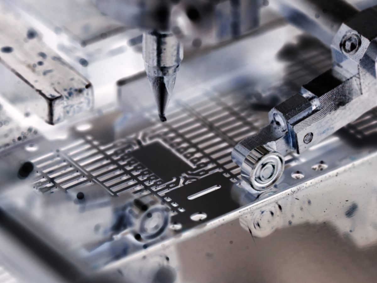
Thermal exposure, residue and material transfer on lead frame carriers, cavity bars, molds and process tooling can make release less predictable and increase cleaning frequency. A surface engineered for lower adhesion and thermal stability helps maintain cleaner release and longer operating intervals.
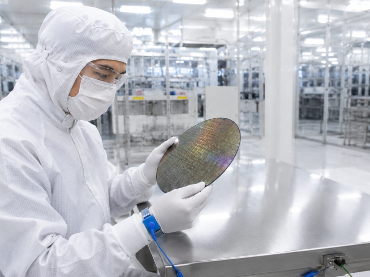
Metrology fixtures, solder ball templates and charge-sensitive handling surfaces need controlled dissipation rather than uncontrolled charge accumulation. The surface requirement is defined around target resistivity, substrate conductivity, grounding path and operating conditions to support stable handling, placement and measurement.
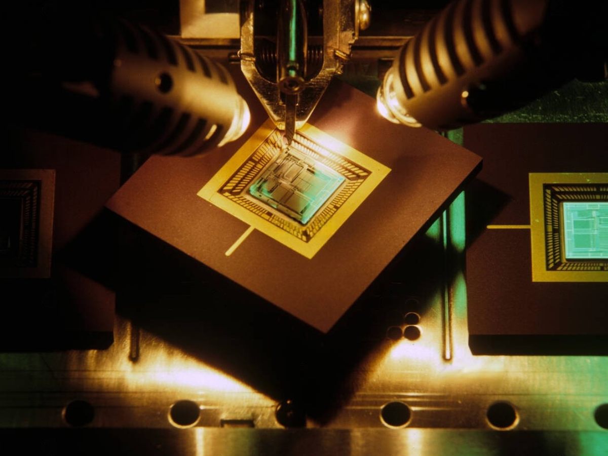
High-contact interfaces can generate debris as surfaces wear, degrade or pick up material. Maintaining a hard, low-friction and stable surface condition helps reduce degradation and material transfer, supporting cleaner interfaces and lower particle-related process risk.
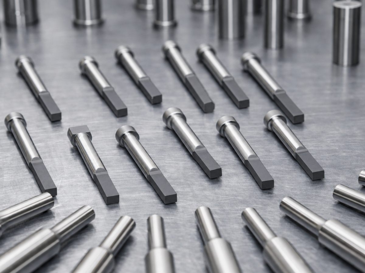
Trim and form, punching and singulation tools rely on edge geometry as contact cycles accumulate. Protecting the working edge while keeping coating build low helps slow burr development, preserve cut quality and reduce inspection or scrap pressure.
Explore selected application examples across metrology, packaging, lapping, bonding and precision tooling to see how surface engineering supports tool life, cleaner release, charge control and process stability.
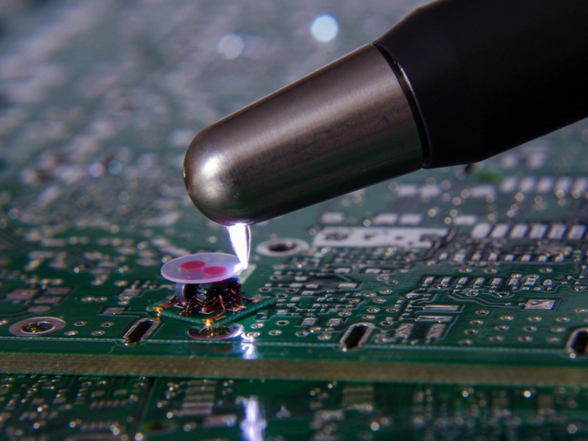
Controlled surface resistivity helps reduce charge accumulation on metrology and test fixtures, supporting more stable handling and measurement conditions around ESD-sensitive devices.
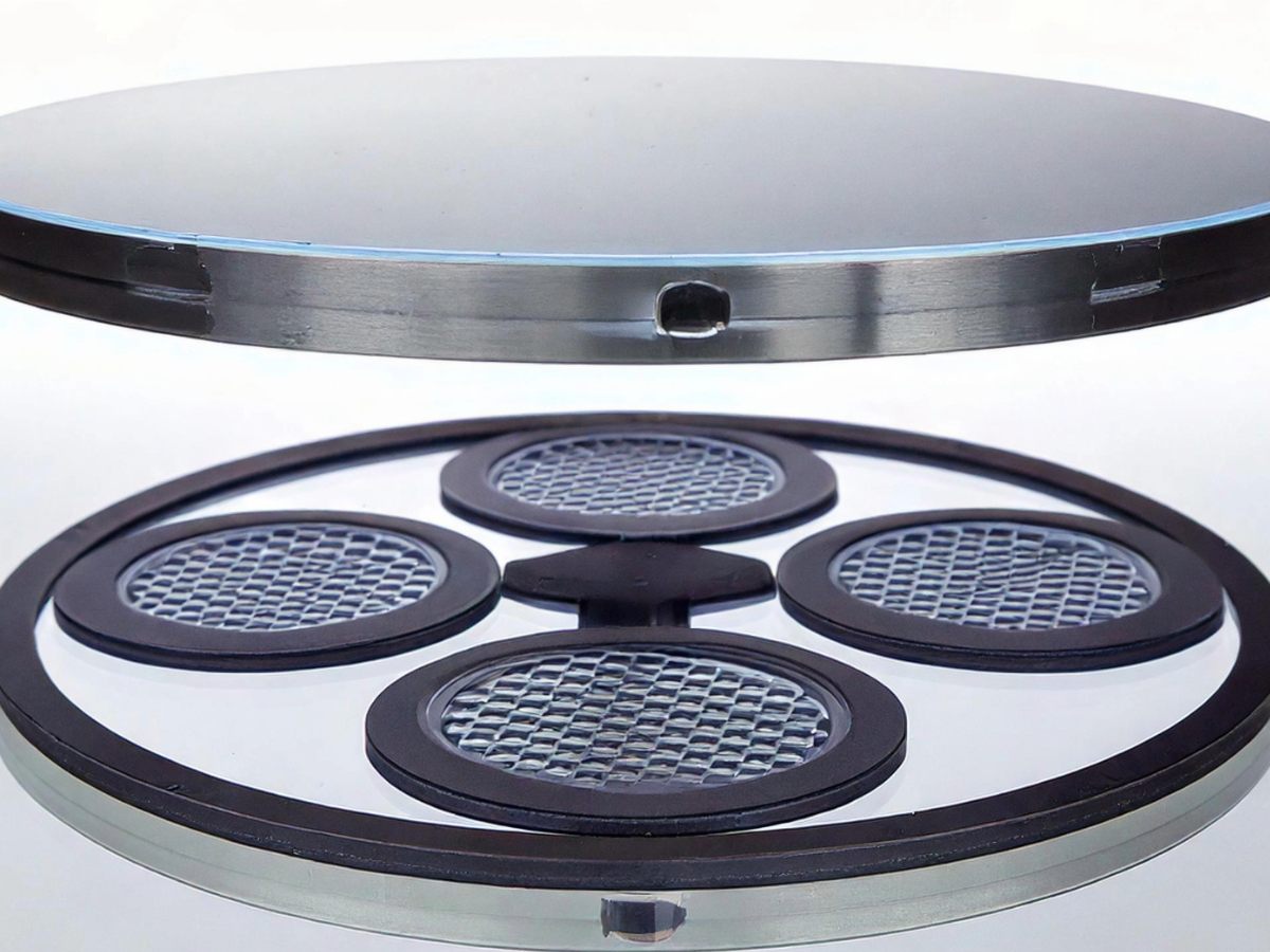
NTI TAC-ON® Protect helps reduce wear that can shift carrier geometry, supporting longer in-spec service life and more consistent lapping conditions.
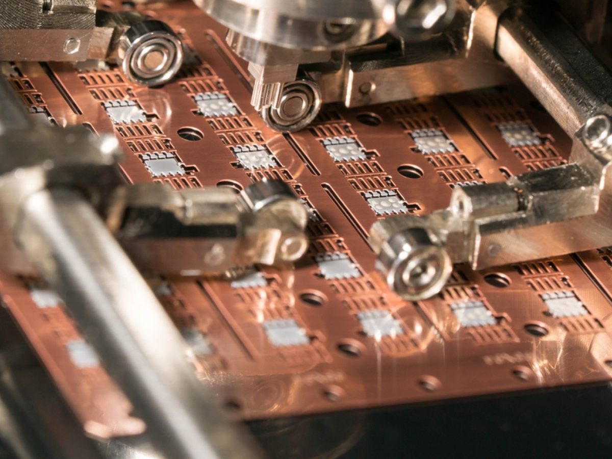
NTI F-TAC™ Protect helps resist material transfer and sticking under thermal exposure, supporting cleaner release, fewer cleaning interventions and longer operating intervals.
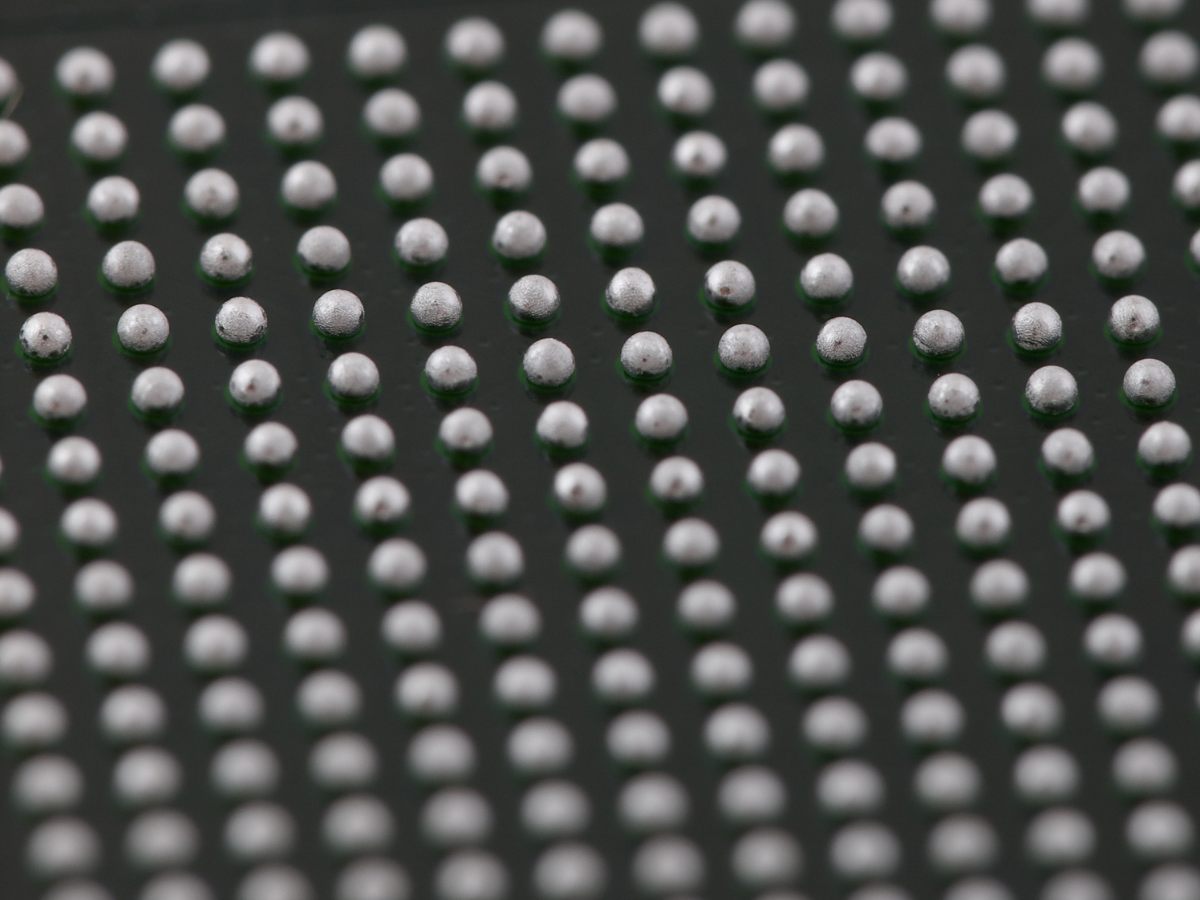
NTI ESD Control coatings help manage surface charge to support cleaner solder ball release and more stable placement in charge-sensitive packaging processes.
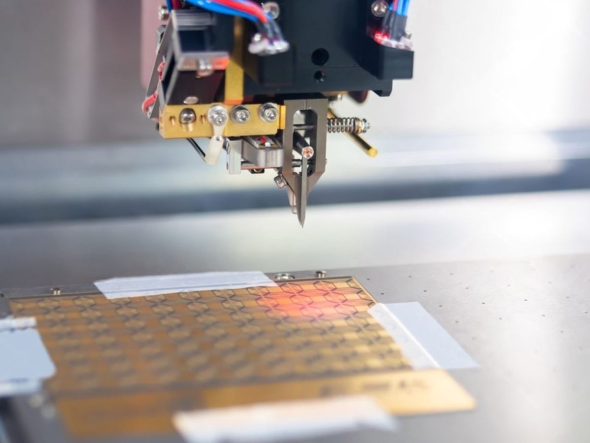
NTI i-TAC® Protect combines wear resistance with thermal stability to help maintain wedge tool condition through repeated ultrasonic and thermal loading.
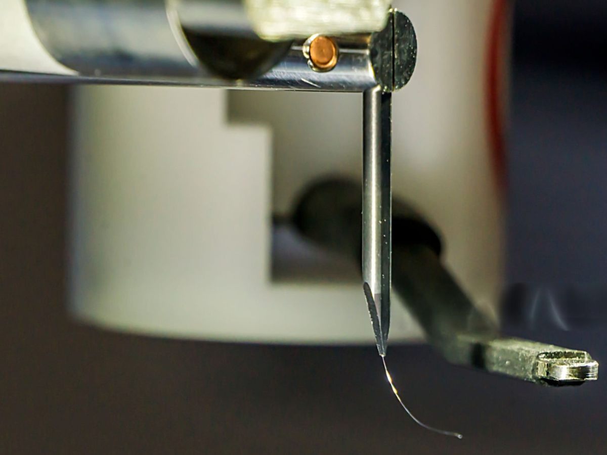
NTI TAC-ON® Protect helps reduce friction and wear on capillary surfaces to help sustain tool condition and bonding consistency through repeated contact.
NTI Nanofilm supports customers through coating services, industrial coating equipment and application development. This gives semiconductor manufacturers, OSATs, component suppliers and equipment makers the flexibility to qualify a solution, localize capability or support future programs with the route that best fits their operation.
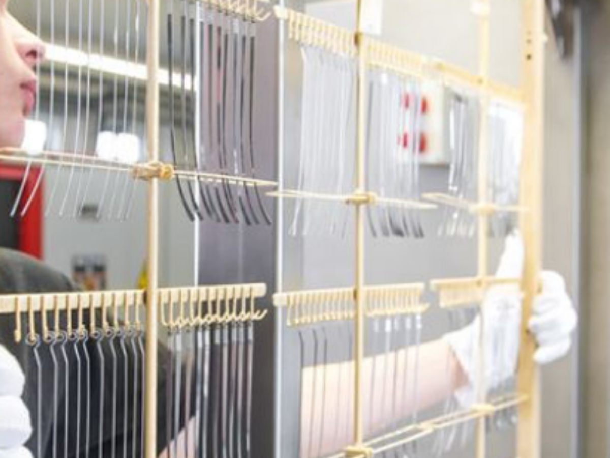
Use NTI Nanofilm coating services to review the application, refine the surface route and support production needs through an established coating network. This route is suited to teams that want surface improvement without adding in-house coating infrastructure.
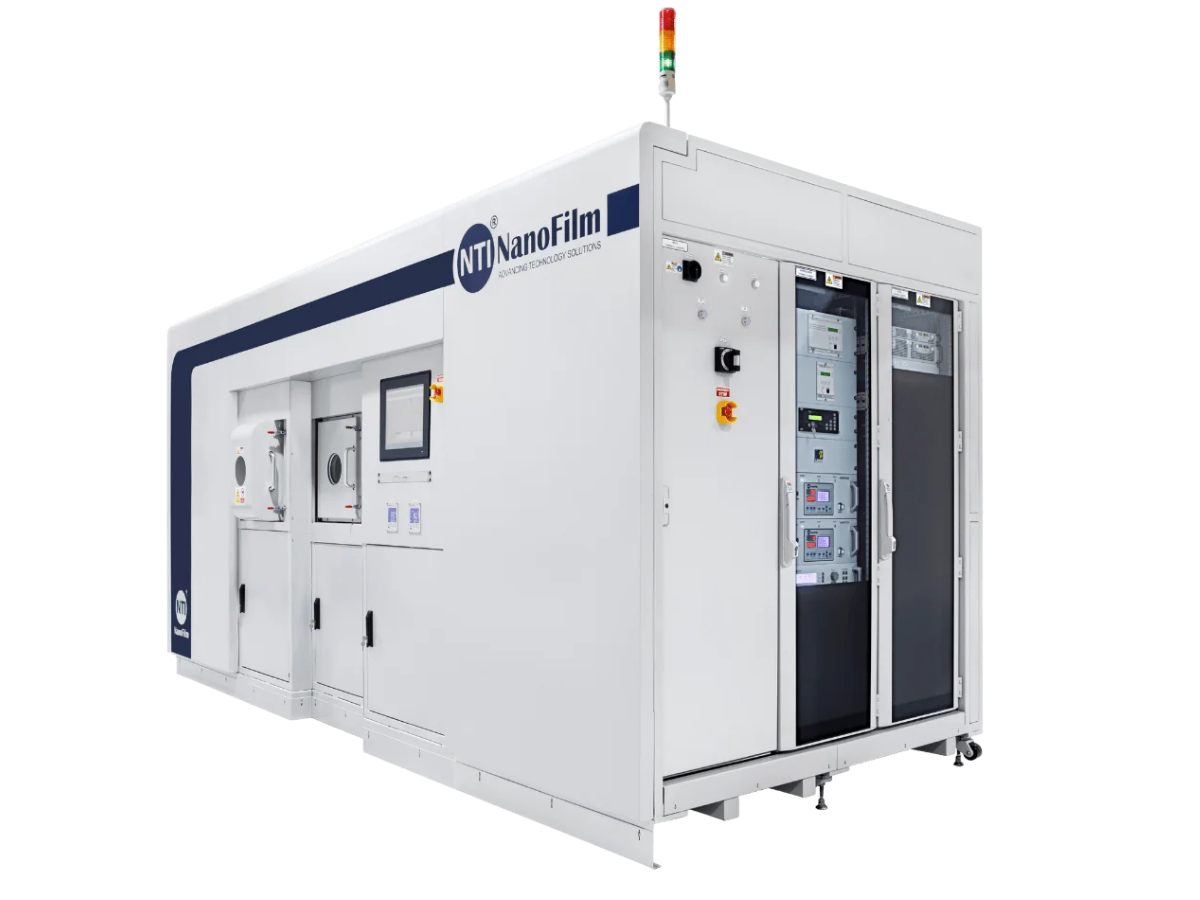
Bring coating capability closer to the production footprint with NTI industrial coating platforms for R&D, batch, load-lock and inline deployment. This route supports customers who want greater control over capacity, process ownership and manufacturing flexibility.

Work with NTI Nanofilm on surface requirements that need more than an off-the-shelf answer. This route supports joint development around emerging tooling, process changes and next-generation manufacturing needs where the surface must be engineered to match the application.
Continue exploring how NTI surface engineering supports other industries through coating technologies, equipment platforms and application development.



Share your application, process conditions and production priorities with NTI Nanofilm. Together, we can identify the surface engineering route that supports longer tool life, cleaner release, controlled ESD, lower particle risk and more consistent production.
NTI Nanofilm supports semiconductor equipment and tooling applications such as lapping carriers, wire bond capillaries, wedge tools, lead frame carriers, solder ball templates, metrology fixtures, test fixtures, trim and form tools, punching tools and singulation tooling. The recommended route depends on the substrate, contact condition, operating temperature, process environment and required surface outcome.
High-contact components can wear over time, affecting geometry, friction and tool condition. NTI surface technologies help reduce surface wear and preserve functional surfaces for longer, supporting longer maintenance intervals, fewer replacements and more stable production performance.
For applications such as lead frame carriers, cavity bars, molds and other thermal-process tooling, NTI F-TAC™ Protect can support anti-stick behavior under heat exposure. NTI MiCC® Hard Protect can also be considered where release performance needs to be combined with hard surface protection.
Yes. NTI ESD Control coatings are suited to applications where controlled surface resistivity is required. On metrology fixtures, solder ball templates and charge-sensitive handling interfaces, controlled resistivity can help reduce charge accumulation and lower ESD-related process risk.
Particles can be generated when high-contact surfaces wear, degrade or pick up material during repeated operation. Hard, low-friction surfaces can help reduce surface degradation and material transfer at selected interfaces, supporting cleaner contact conditions and longer intervals between maintenance interventions.
NTI RainbowTAC™ Protect is suited to precision cutting applications where edge condition and dimensional control matter. Its ultra-thin, high-hardness layer helps protect working edges, supporting cleaner cuts and slower burr development over time.
Yes. Customers can work with NTI Nanofilm through production coating services, industrial coating equipment or joint application development. This gives semiconductor manufacturers and equipment suppliers flexibility to outsource coating production, localize coating capability or develop a new surface route around future process needs.
The review starts with the component, substrate, surface condition, contact mode, temperature, process chemistry and target performance outcome. From there, NTI can recommend a relevant surface route and a validation plan around the properties and application conditions that matter most for the component.
Enabling more reliable semiconductor manufacturing through advanced coatings for critical tools and carriers.
As semiconductor devices become more advanced, manufacturers face growing challenges in precision, durability, contamination control, and cost efficiency. Traditional coatings often fall short in addressing equipment wear, electrostatic discharge (ESD), and surface degradation, leading to higher maintenance costs, reduced yield, and process inefficiencies.
NTI Nanofilm offers cutting-edge DLC (Diamond-Like Carbon) and nanocomposite coatings powered by our proprietary Filtered Cathodic Vacuum Arc (FCVA) technology. Our coatings provide exceptional hardness, ultra-low friction, superior adhesion, and enhanced thermal and chemical resistance—meeting the demanding needs of semiconductor production.
High-hardness, low-friction coatings improve wear resistance and dimensional stability, reducing edge chipping and friction variation while extending service life and maintaining consistent grinding performance.
High-temperature, anti-stick coating structures help reduce metal adhesion and thermal fatigue risk, minimize cleaning-related downtime, and support stable operation at high production throughput.
Enhanced oxidation and wear resistance help stabilize friction behavior and geometric accuracy during bonding, reducing tool replacement frequency and improving bonding consistency.
Protects lead frames during reflow and baking processes, reducing adhesion, cleaning frequency, and downtime.
Extends the service life of wire bonding tools, improves adhesion performance, and reduces maintenance requirements.
Prevents static charge buildup on solder ball stencils, enabling clean and precise solder ball placement.
Improves the durability of grinding carriers, reduces replacement frequency, and helps maintain wafer consistency.
Allows ceramic components to be coated without a metallic layer, helping minimize particle shedding and wear.
Protects elastomer seals from plasma and corrosive gas attack, extending service life and maintaining chamber cleanliness.

Do you have any question and want to know more about our services? We will be glad to support you.
NTI Nanofilm’s advanced thin-film coatings address key semiconductor manufacturing challenges such as equipment wear, contamination, electrostatic discharge (ESD), and process inefficiencies. Our DLC (Diamond-Like Carbon), fluorinated coatings, and nano-crystalline coatings enhance durability, reduce defects, and extend component lifespan—ensuring higher yield, cost efficiency, and process reliability.
Our proprietary Filtered Cathodic Vacuum Arc (FCVA) technology delivers ultra-dense, high-purity thin-film coatings with superior hardness, low friction, and excellent adhesion. Unlike traditional PVD or CVD coatings, FCVA produces smooth, contamination-resistant surfaces ideal for lapping carriers, wafer e-chucks, lead frames, and wire bonding tools, improving manufacturing efficiency and reducing downtime.
TAC-ON® (Tetrahedral Amorphous Carbon) coatings provide exceptional hardness, wear resistance, and ultra-low friction, extending the lifespan of critical wafer processing and packaging components. They help reduce defects, minimize contamination, and optimize semiconductor manufacturing yields, making them ideal for high-precision applications.
Our ASD (Anti-Static Discharge) coatings offer customizable surface resistivity (10⁵–10⁹ Ohms/sq), protecting sensitive semiconductor tools, lead frames, and wafer carriers from electrostatic discharge damage. By preventing static buildup and particle contamination, ASD coatings enhance component reliability, yield stability, and manufacturing efficiency.
NTI Nanofilm’s high-performance thin-film coatings extend equipment lifespan, reduce maintenance costs, improve process consistency, and minimize material waste. Our solutions help semiconductor manufacturers reduce total cost of ownership (TCO) by optimizing equipment performance, yield enhancement, and defect reduction, leading to higher operational efficiency and cost savings.