Advanced Thin-Film Coatings for Through-Silicon Vias (TSV) and Through-Glass Vias (TGV)


Contact Us


TSV & TGV: The next leap in IC packaging

As IC packaging evolves from traditional wire bonding to silicon and glass interposers, Through-Silicon Vias (TSV) and Through-Glass Vias (TGV) have become central to system-level performance scaling. The rapid rise of AI/HPC accelerators, HBM integration, and mmWave applications is driving widespread adoption of 2.5D/3D architectures and panel-level glass substrates, pushing via dimensions deeper and narrower than ever before. 

This shift concentrates electrical and mechanical stress at the interposer, making high-aspect-ratio metallization, diffusion blocking, and long-term thermal reliability critical to yield and cost control.

Packaging approach What it enables Where demand is
2.5D with TSV Ultra-bandwidth, low-latency links for 2.5D/3D AI/HPC, HBM on GPU/ASIC, networking
Panel glass with TGV Low-loss RF paths + panel-level scaling 5G/mmWave, radar, photonics/optics
Fan-Out (FO-WLP) Thin form factor, high-density RDL Mobile & edge AI (growing)
SiP / Heterogeneous Mix logic/RF/MEMS/power in one module IoT, automotive mid-tier (growing)
Flip-Chip Short interconnects, high I/O CPUs/SoCs (stable)
WLCSP Wafer-level, ultra-small footprint Sensors & small ICs (niche)
Wire Bonding Long wires, low I/O, low cost Legacy/cost-sensitive (mature)

Packaging approach Driving TSV & TGV Adoption

IC packaging now ranges from legacy wire bonding to advanced 2.5D/3D interposers, with TSV driving AI/HPC and HBM systems and TGV gaining momentum in 5G, mmWave, and photonics. Fan-out and heterogeneous SiP are expanding in mobile and automotive markets, while flip-chip, WLCSP, and wire bonding remain stable in cost-sensitive applications.

High-Aspect-Ratio (AR) Metallization Challenges


  • Critical Coating Requirements

    TSV and TGV manufacturing demand barrier, adhesion, and seed layers to be deposited uniformly.

  • Process
    Limitations

    Conventional approaches struggle with coverage, speed, and reliability in AR > 5:1 features.

  • Impact on Manufacturing Economics

    These limitations translate into yield loss, increased cost, and greater integration complexity.

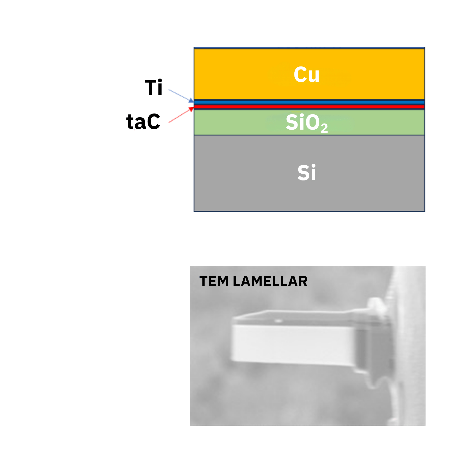
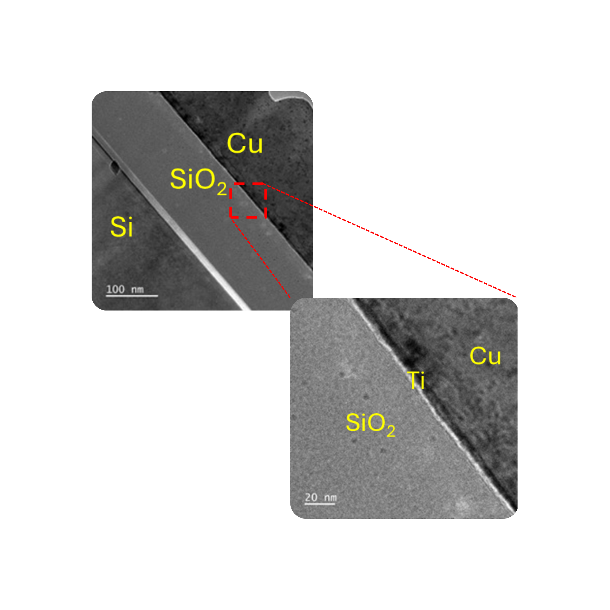
The Critical Role of FCVA Coatings in TSV/TGV

TSV and TGV manufacturing demands super-conformal barrier and seed layers with strong adhesion, low stress, and defect-free coverage capabilities that conventional PVD, wet plating repair, or slow ALD stacks struggle to deliver economically at scale.

NTI Nanofilm’s proprietary Filtered Cathodic Vacuum Arc (FCVA) technology uniquely combines:
- High-AR via coverage with ion-assisted adhesion
- Dense, pinhole-free ta-C / DLC barrier layers
- Low-temperature deposition (<100 °C)
- Single-tool barrier + seed capability 

These attributes help fabs simplify process flows, improve plating yields, and protect reliability during thermal cycling unlocking scalable TSV/TGV integration for next-generation packages.

TGV FCVA

FCVA Deposits Both Barrier and Seed Layers in High-AR Vias

Enables single-tool deposition of both barrier and seed layers, reducing process steps, improving yield.

  • Test Structure Containing 1 nm ta-C

  • X-TEM & ToF-SIMS confirms no Cu diffusion through 1 nm ta-C between Ti and SiO₂ after high-temp annealing at 600oC for 40 min

Unlocking Performance, Yield, and Cost Advantages with FCVA

  • Environmental Compliance

    Dry vacuum process eliminates hazardous wet-chemical waste.

  • Improved Via Yield

    Reliable conformality in deep vias reduces plating voids and rework.

  • Scalable Manufacturing

    Wafer-ready today with pathways to panel-level production.

  • Process Simplification

    Single-tool barrier/seed deposition cuts steps, cycle time, and total cost of ownership.

  • Enhanced Reliability

    Dense diffusion barriers and strong interfaces resist delamination and Cu migration during thermal cycling.

  • Low-Temperature Compatibility

    Supports glass substrates and advanced integration stacks.

Choosing the right route for superconformal deep-via barrier/seed

Comparing deposition routes for deep-via barrier/seed, FCVA uniquely combines high-AR via coverage, ion-bonded adhesion, pinhole-free density, and <100 °C deposition in one clean vacuum step.

Capability PVD (Sputtering) Electroless Plating ALD/CVD (Chemical Deposition) NTI Nanofilm FCVA
Step coverage in high-AR vias Limited (≈≤5:1) Good; repairs seed but low density ALD: excellent
CVD: better than PVD
Excellent + dense in high AR
Adhesion to glass/silicon Moderate Variable (activation-dependent) Good with surface prep High (ion implantation, graded interface)
Film density & barrier quality Moderate Low–medium (NiP/Cu) ALD: high-density liners 
CVD: medium–high
High, pinhole-free (ta-C ~3.3 g/cm³)
Deposition temperature Low (<200 °C) Low ALD: low–med (<200 °C) 
CVD: med–high (>300 °C)
Low (<100 °C)
Throughput & thickness feasibility Fast for thin; struggles conformal thick Good rate; conformal; adds wet steps ALD: very slow >50 nm
CVD: moderate-fast
High rate (thin–mid); single tool
Process complexity Often needs electroless repair Multi-bath + waste treatment Often paired with PVD/seed Single-step capable
Environmental footprint Low–medium High (wet chem waste) Low–medium (precursor/abatement) Low (dry vacuum)
Reliability under thermal cycling Thin-spot/seed delam risks Adhesion variability Good liners; stack-dependent Strong adhesion; dense barriers resist diffusion

Ready to get started?

Do you have any question and want to know more about our services? We will be glad to support you.

Contact Us

We use cookies on our website to see how you interact with it. By accepting, you agree to our use of such cookies. Cookie Policy