Thin, lightweight optical structures support compact sensing and light management while keeping geometry and integration aligned with wearable form factors.

Advance the next generation of compact devices with polymer optics engineered for both optical performance and high-volume production. NanoFab connects optical design, DFM, precision mastering and replication to support stronger yield, smoother production transfer and lower total cost per part.
Smaller devices, denser sensing architectures, smarter wearables and in-cabin systems are demanding more from polymer optics as launch volumes and cost pressures rise. Light control, optical geometry and compact integration now have to be balanced with manufacturability, yield and total cost. Integrating optical design, master tooling and replication earlier helps reduce late-stage redesign, protect optical intent and improve production readiness.
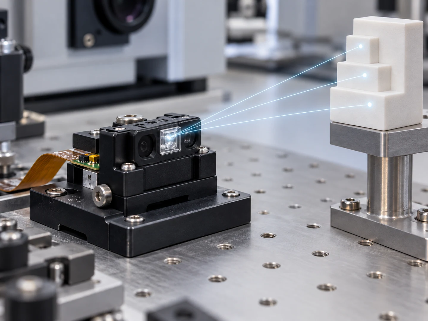
Illumination, sensing and light-management functions are becoming more demanding as optical systems take on more responsibility within the final device.
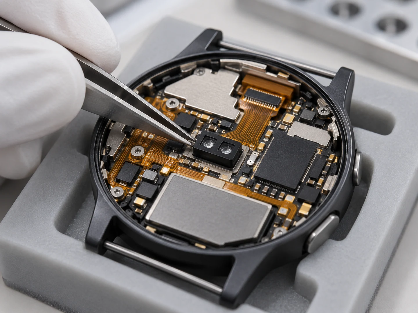
Compact form factors place tighter limits on geometry, package integration and assembly, increasing the need to consider manufacturability earlier.
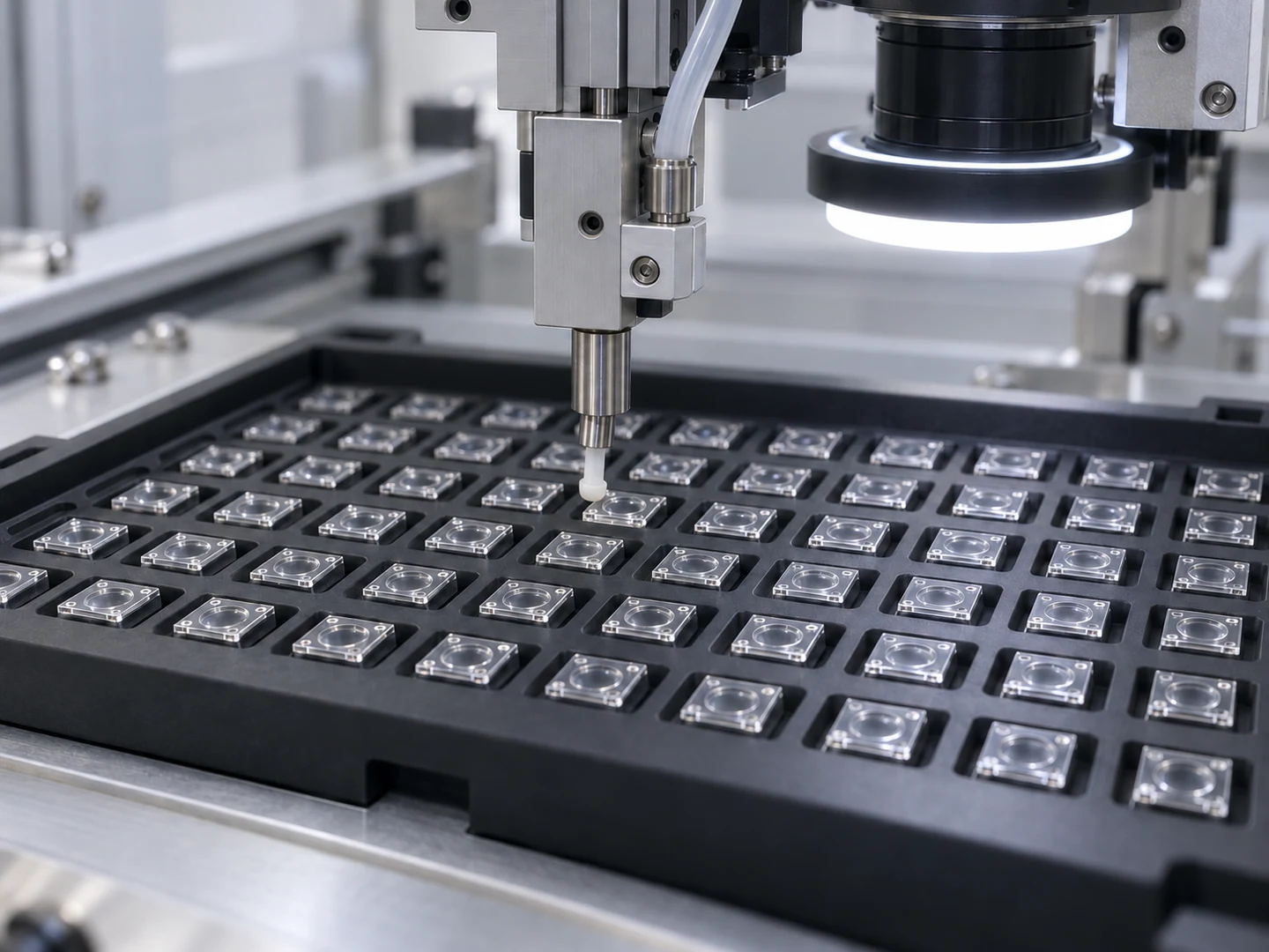
Production programs need optical quality to hold as output increases, with yield, cycle efficiency and total cost per part becoming as critical as optical performance.
NanoFab brings DFM, precision mastering, tooling, nanoimprint or molding and production control into one connected platform. Start with Design-to-Production when the optic still needs to be developed around the application, or move into Build-to-Print when the optical design is already established.
Whether your optical design is already defined or still needs to be developed, NanoFab helps connect the critical steps earlier so fewer issues surface later. By bringing design, DFM, tooling, replication and production closer together, you can protect optical intent, reduce unnecessary iteration and improve yield, consistency and cost control at higher output.
Start from an established optical design and align DFM, tooling and manufacturing requirements earlier. This helps reduce avoidable redesign, improve tooling readiness and move the optic into repeatable production with fewer downstream surprises.
Translate optical performance, geometry and integration requirements into a production-ready design before tooling begins. This helps shorten the distance between application intent and a manufacturable optic that can progress into volume production.
Bring DFM, master tooling, nanoimprint and molding into a more connected manufacturing flow. Fewer disconnected handoffs help preserve geometry, reduce interpretation gaps and improve consistency from optical design through replicated parts.
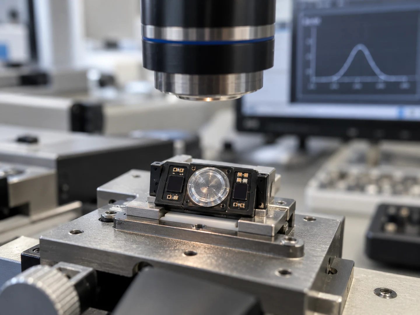
Use established process control to maintain optical quality as production volumes increase. Stronger manufacturing yield, more consistent output and tighter cost control help qualified polymer and micro-optics programs perform more competitively in recurring production.
Assembly integration, functional coatings and validation can be brought closer to the optics manufacturing flow to reduce handoffs, simplify downstream assembly and carry more of the finished-component requirement within one coordinated production program.
Move optical geometry from master tooling into high-volume polymer optics through 5-axis diamond turning, nanoimprint lithography and micro injection molding. NanoFab brings together the technologies, software and production capabilities needed to preserve optical form, support repeatable output and lower total cost in manufacturing.
Generate freeform, Fresnel and microlens master geometries in-house with 5-axis single point diamond turning supported by proprietary CAM software. Closer control over tool path and master form helps preserve optical geometry earlier, reduce rework before replication and prepare the optic more effectively for downstream tooling.
Replicate fine microstructured and reflowable optical geometries into polymer with nanoimprint lithography. The process supports thin, lightweight optical structures while helping maintain feature consistency, improve replication efficiency and keep unit cost competitive in higher-volume manufacturing.
Produce complex three-dimensional polymer optical geometries through repeatable micro injection molding cycles. Tool-based replication combines geometric freedom with cycle-time efficiency, helping support stable output, higher yield and commercially competitive volume production.
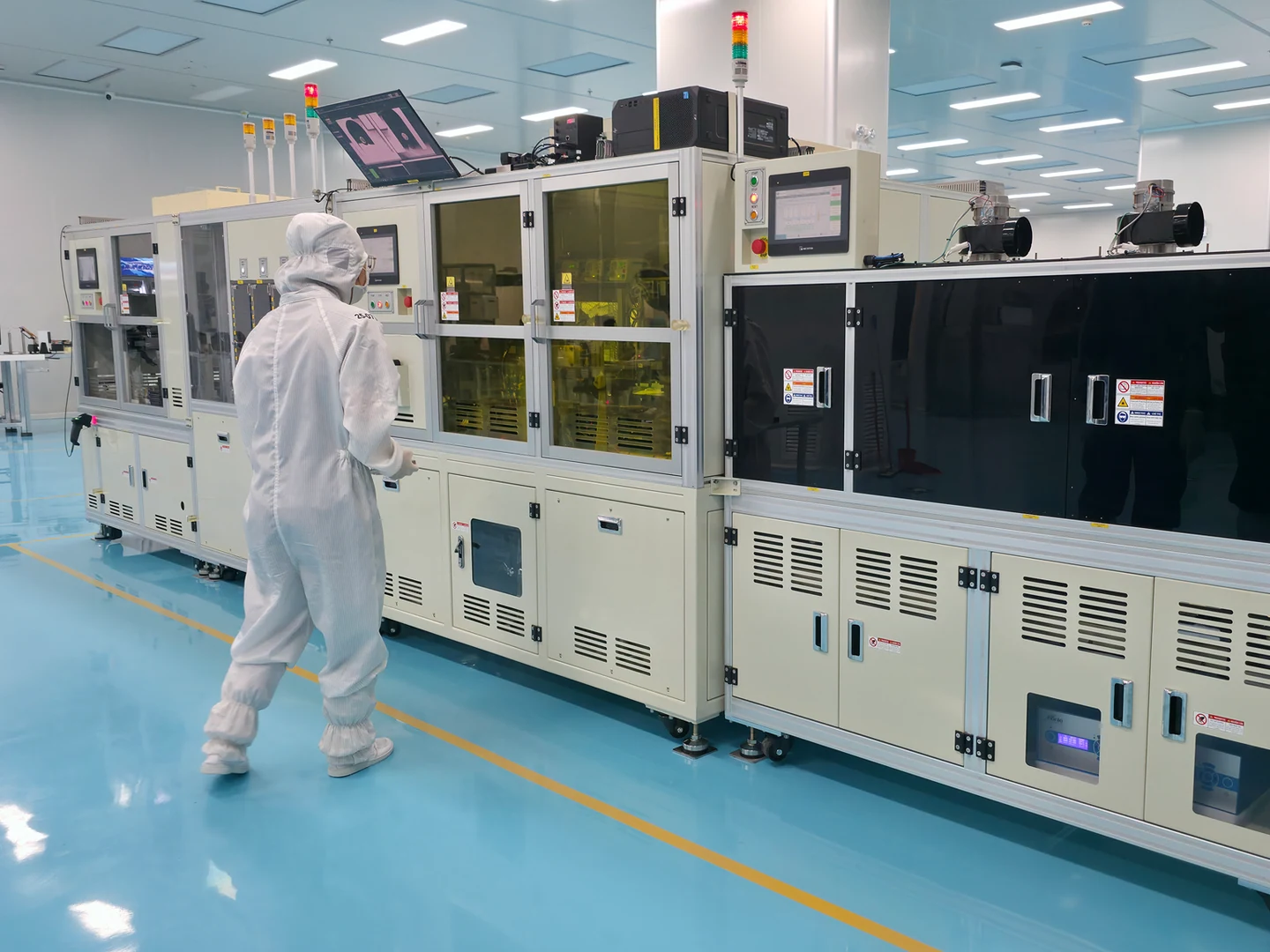
NanoFab combines more than 35,000 sqm across production and expansion capacity with output capability of up to 20 million parts per month, subject to design and process. This supports higher-volume polymer optics programs with the manufacturing room needed for recurring output and future growth.
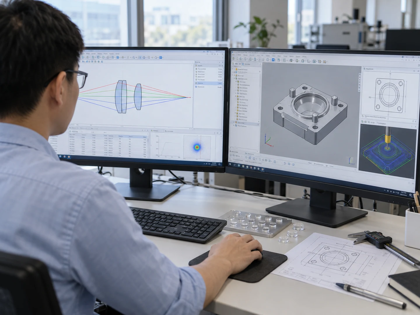
Connect optical, mechanical, CAM, automation and vision software more closely with tooling and production control. Platforms such as Zemax OpticStudio, LightTools, SolidWorks, AutoCAD, LabVIEW and production automation tools help shorten iteration, improve geometry transfer and support more consistent manufacturing execution.
Illumination, sensing, light coupling and wearable optics each place different demands on geometry, optical efficiency, packaging, durability and production volume. NanoFab brings optical design and polymer manufacturing together so the optic can be engineered around how light needs to behave in the final device, while remaining practical to integrate and manufacture at volume.

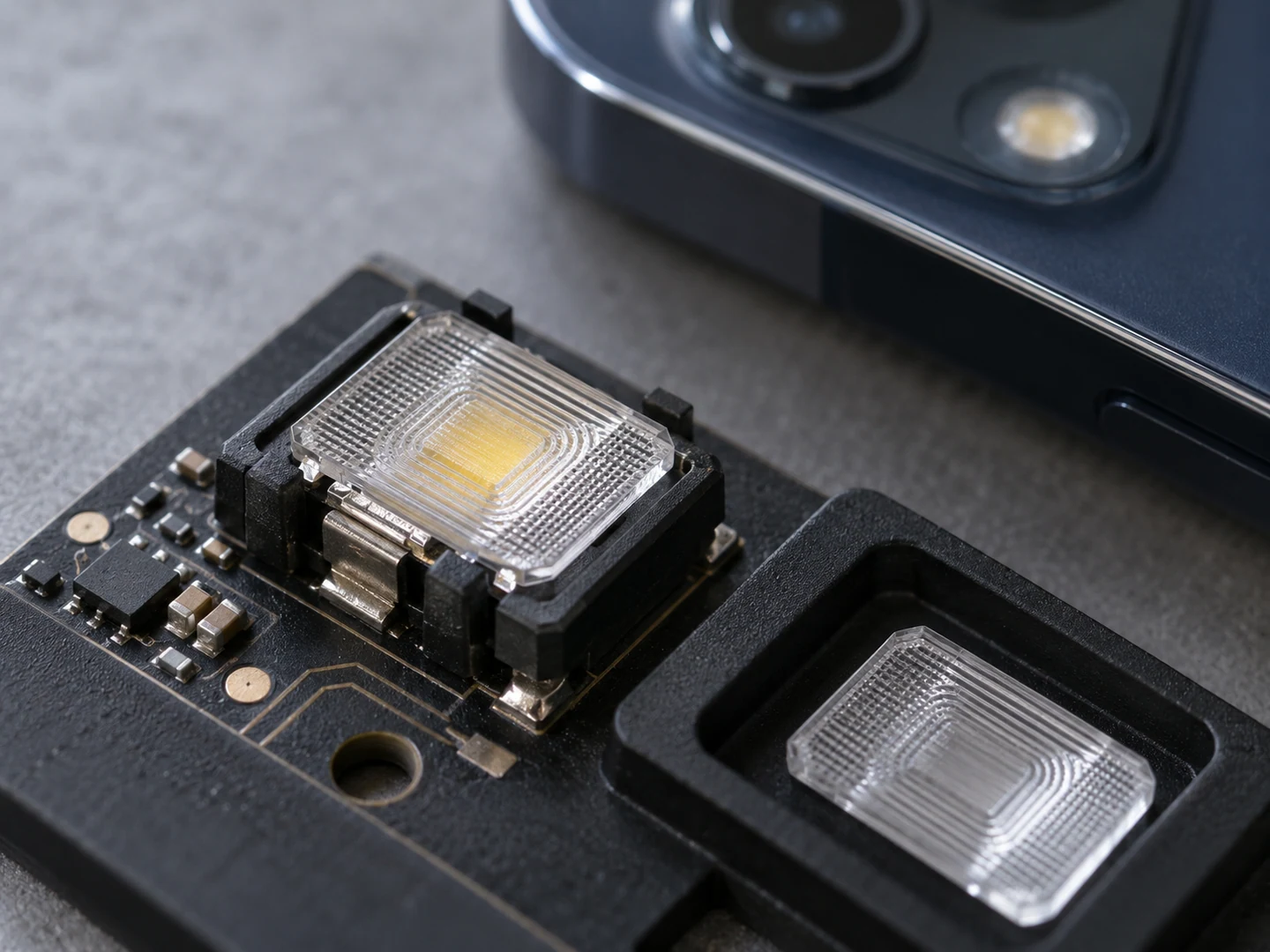
Precision polymer optics support controlled illumination, sensing and light management in compact devices, helping consumer programs improve yield, consistency and cost competitiveness.

Polymer optics support sensing and illumination functions where geometry, integration, durability and repeatable output need to come together for automotive production.

Thin, lightweight optical structures support compact sensing and light management while keeping geometry and integration aligned with wearable form factors.

High-precision coupling optics support denser optical connectivity architectures, where compact geometry, signal quality and manufacturing consistency all matter.

Polymer optics for ToF and 3D sensing support depth perception and compact integration while enabling repeatable output for higher-volume robotic platforms.

In-cabin sensing optics support driver monitoring accuracy, system integration and production readiness for automotive interior sensing applications.
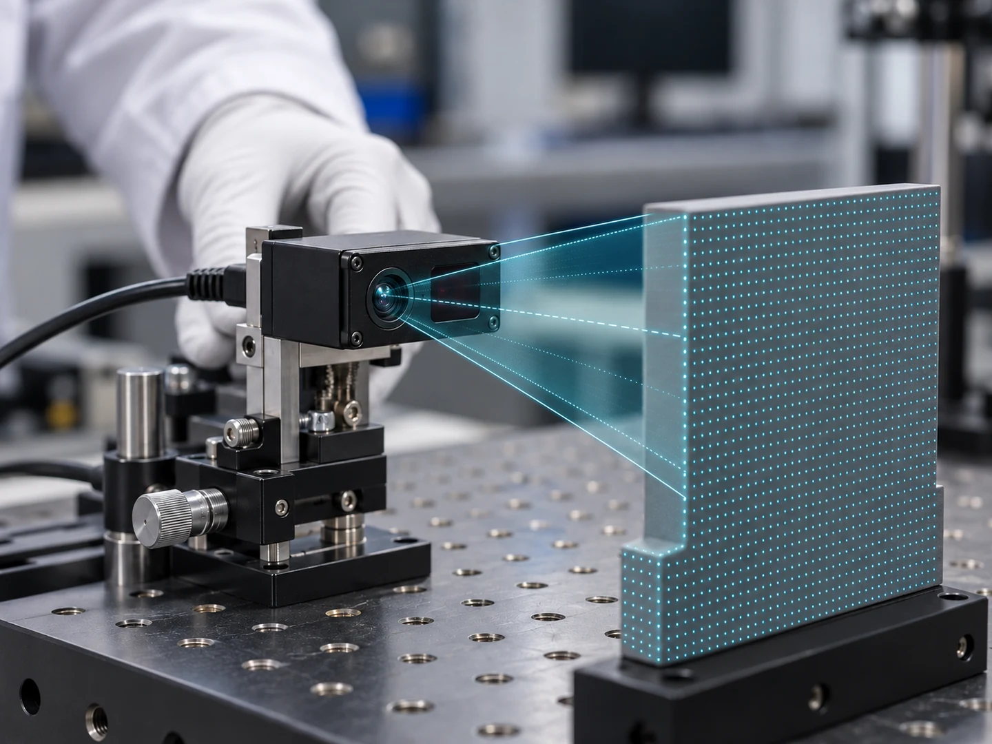
Micro-optics help shape, direct and collect light for structured light and time-of-flight architectures that require repeatable geometry transfer.

Compact optics support health-sensing modules where profile matching, package integration and reliable output are important to the finished device.
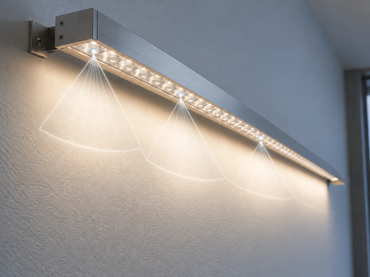
Polymer optics support beam shaping, diffusion and light-guiding functions where optical performance and manufacturing practicality need to be aligned together.
Precision optics are critical to product performance, reliability and user experience. Through OEM manufacturing and ODM design support, NanoFab turns optical requirements into production-ready polymer optics that scale with consumer demand.
Parts shipped to-date
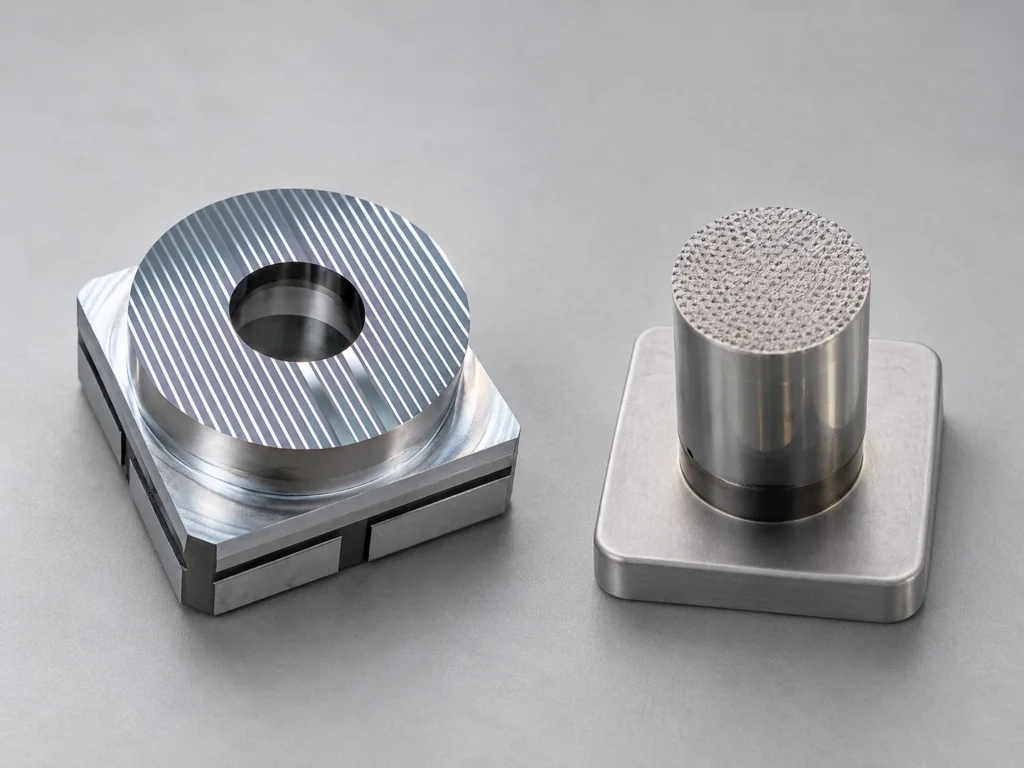
A durable metal master strengthened lens form and surface quality while supporting production of more than 100 million nanoimprinted parts, showing how stronger master generation can carry optical quality further into high-volume replication.

Bring your optical design, application requirement, geometry, material, performance target or production volume. NanoFab can help identify the right path through NF Fab™ or NF Design+™ and move the program toward reliable, high-volume polymer and micro-optics manufacturing.
NF Fab™ is NanoFab’s Build-to-Print pathway for OEM Manufacturing. It is suited to programs where the optical design is already established and needs to move through DFM, tooling and high-volume production. NF Design+™ is NanoFab’s Design-to-Production pathway for ODM Manufacturing. It begins earlier with optical design, then carries the program through DFM, master tooling and production.
Build-to-Print is a strong fit when the optical design or print is already defined and the next priority is industrialization. NF Fab™ helps align that design with DFM, tooling, nanoimprint or micro injection molding and the process discipline needed for repeatable high-volume output.
Design-to-Production is the broader pathway when the application requirement is clear but the optical solution still needs to be developed. NF Design+™ helps translate optical performance, geometry and integration requirements into a manufacturable design and then carries the same program through tooling and production.
NanoFab supports a range of polymer and micro-optical structures including freeform optics, Fresnel optics, microlens geometries and other optical features used for illumination, sensing, light coupling and wearable applications. The appropriate manufacturing path depends on optical geometry, replication method, integration needs and production volume.
Yes. DFM is part of both NF Fab™ and NF Design+™. NanoFab also supports master generation and tooling capabilities, helping connect optical intent more closely with downstream replication and production requirements.
Core capabilities include 5-axis single point diamond turning, nanoimprint lithography and micro injection molding, supported by production and software capabilities. The appropriate technology path depends on geometry, optical function, integration needs and the intended production volume.
Yes. NanoFab can incorporate assembly integration features, functional coatings and validation support closer to the optics manufacturing flow. This can help reduce handoffs, simplify downstream assembly and improve confidence before deeper production release.
NanoFab commonly supports applications across consumer electronics, automotive, smart eyewear, AI and datacenter optics and robotics. Across these sectors, the emphasis is on aligning optical performance with integration needs and production readiness.
Production capability depends on part geometry, process flow and the qualified manufacturing path. NanoFab supports recurring high-volume output, with additional capacity available for qualified programs as production requirements increase.
Share the optical design, application requirement, geometry, material, performance target or anticipated production volume through the discussion form. NanoFab can then help determine whether NF Fab™ or NF Design+™ is the more suitable starting path.